- STMicroelectronics Community
- STM32 MCUs
- STM32 MCUs products
- stm32vl discovery layout
- Subscribe to RSS Feed
- Mark Topic as New
- Mark Topic as Read
- Float this Topic for Current User
- Bookmark
- Subscribe
- Mute
- Printer Friendly Page
stm32vl discovery layout
- Mark as New
- Bookmark
- Subscribe
- Mute
- Subscribe to RSS Feed
- Permalink
- Email to a Friend
- Report Inappropriate Content
2011-02-27 04:03 PM
Hi,
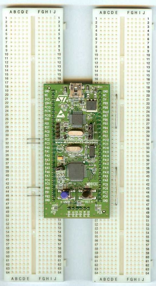
I want to use the board on top of a ''motherboad'', so I need STM32 VL Discovery layout (or just P1, P2 and P3 layout dimensions), where can I find it? thanks in advance.- Mark as New
- Bookmark
- Subscribe
- Mute
- Subscribe to RSS Feed
- Permalink
- Email to a Friend
- Report Inappropriate Content
2011-02-27 07:08 PM
Pretty sure you'll find it's all set up with a 0.1'' pitch in both X/Y so you can stick it on a proto/vero board. Would be easy to verify.
http://www.djerickson.com/stm32/Up vote any posts that you find helpful, it shows what's working..
- Mark as New
- Bookmark
- Subscribe
- Mute
- Subscribe to RSS Feed
- Permalink
- Email to a Friend
- Report Inappropriate Content
2011-03-08 03:51 PM
''Pretty sure you'll find it's all set up with a 0.1'' pitch in both X/Y''
Yes, it is''so you can stick it on a proto/vero board.''
Yes, you can The only question is: what to do about that pesky row of pins along the bottom?! Here's what I did:

- Mark as New
- Bookmark
- Subscribe
- Mute
- Subscribe to RSS Feed
- Permalink
- Email to a Friend
- Report Inappropriate Content
2011-03-24 03:59 PM
We are using the long protoboards from dipmicro.com with strip sockets. The boards are high quality, plated through FR4 with solder mask.
Because they are designed for SMT DIPS with 0.05'' spacing, the outer set of contacts are separate from the inner sets, so you can use 0.1'' parts under the Discovery board without conflict. You can handle the end contacts most easily by not installing a socket strip, but it was just a minute or two of effort to cut the traces between holes at the end.- Mark as New
- Bookmark
- Subscribe
- Mute
- Subscribe to RSS Feed
- Permalink
- Email to a Friend
- Report Inappropriate Content
2011-03-25 12:10 AM
''the long protoboards from dipmicro.com''
You mean this:http://dipmicro.com/store/PCB-PB4
?
- Mark as New
- Bookmark
- Subscribe
- Mute
- Subscribe to RSS Feed
- Permalink
- Email to a Friend
- Report Inappropriate Content
2011-03-25 04:29 AM
Always preferred pad-per-hole wire-wrap my self.
http://www.futurlec.com/ProtoBoards.shtml
Up vote any posts that you find helpful, it shows what's working..
- Mark as New
- Bookmark
- Subscribe
- Mute
- Subscribe to RSS Feed
- Permalink
- Email to a Friend
- Report Inappropriate Content
2011-03-25 05:34 AM
- Mark as New
- Bookmark
- Subscribe
- Mute
- Subscribe to RSS Feed
- Permalink
- Email to a Friend
- Report Inappropriate Content
2011-03-28 12:52 AM
One advantage of a ''pad-per-hole'' board is when you have both ''horizontal'' & ''vertical'' rows of pins - as on the Discovery board...
- STM32F411RE - cannot find schematic sheets anymore in STM32 MCUs products
- what the difference between STM32F407VET6 and STM32F407VGT6 in STM32 MCUs products
- U5 DSI Communications Issues in STM32 MCUs products
- STM32H7 without SMPS - VCAP / LDO ? in STM32 MCUs products
- Failed to erase memory, but flashing possible with TouchGFX Designer and STM32CubeIDE. in STM32CubeProgrammer (MCUs)