Turn on suggestions
Auto-suggest helps you quickly narrow down your search results by suggesting possible matches as you type.
Showing results for
- STMicroelectronics Community
- STM32 MCUs
- STM32 MCUs products
- Missing SDNWE signal using STM32F469NI and SDRAM o...
Options
- Subscribe to RSS Feed
- Mark Topic as New
- Mark Topic as Read
- Float this Topic for Current User
- Bookmark
- Subscribe
- Mute
- Printer Friendly Page
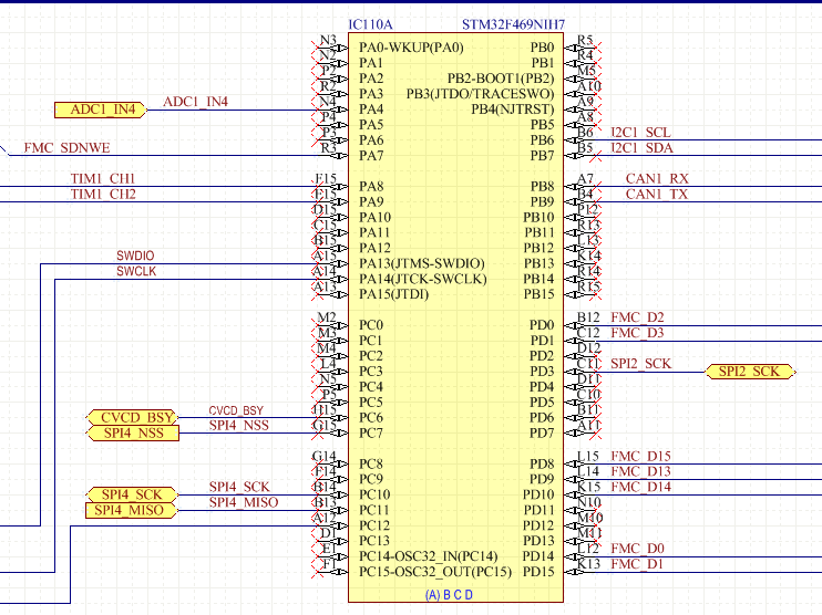
Missing SDNWE signal using STM32F469NI and SDRAM on PA7
Options
- Mark as New
- Bookmark
- Subscribe
- Mute
- Subscribe to RSS Feed
- Permalink
- Email to a Friend
- Report Inappropriate Content
2016-10-06 07:01 AM
Posted on October 06, 2016 at 16:01
The original post was too long to process during our migration. Please click on the attachment to read the original post.
Solved! Go to Solution.
1 ACCEPTED SOLUTION
Accepted Solutions
Options
- Mark as New
- Bookmark
- Subscribe
- Mute
- Subscribe to RSS Feed
- Permalink
- Email to a Friend
- Report Inappropriate Content
2017-08-01 08:44 AM
Posted on August 01, 2017 at 17:44
Hello,
Please note that the limitation is described in
as following:Title: FMC_SDNWEN alternate function on PA7
Description
The FMC_SDNWEN alternate function is not available on PA7.
Workaround
Use FMC_SDNWEN alternate function on PH5 or PC0.
A request will be raised internally to take into consideration this limitation in STM32CubeMX.
-Amel
To give better visibility on the answered topics, please click on Accept as Solution on the reply which solved your issue or answered your question.
8 REPLIES 8
Options
- Mark as New
- Bookmark
- Subscribe
- Mute
- Subscribe to RSS Feed
- Permalink
- Email to a Friend
- Report Inappropriate Content
2016-10-06 07:47 AM
Posted on October 06, 2016 at 16:47
> Note that in other examples, SDNWE is mapped to PC0, but this was not possible in this design. According to the datasheet, PA7 should also work for SDNWE.
Just as an experiment, could you try to map SDNWE either to PC0 or PH5? The SDRAM won't work but you could at least check if there is any activity on those pins. JWOptions
- Mark as New
- Bookmark
- Subscribe
- Mute
- Subscribe to RSS Feed
- Permalink
- Email to a Friend
- Report Inappropriate Content
2016-10-06 01:10 PM
Posted on October 06, 2016 at 22:10
Unfortunately, this is not possible in this design because the STM32 in question is in a BGA package and the other alternate pins are not accessible because they are not fanned out. :(
Options
- Mark as New
- Bookmark
- Subscribe
- Mute
- Subscribe to RSS Feed
- Permalink
- Email to a Friend
- Report Inappropriate Content
2016-10-07 01:31 AM
Posted on October 07, 2016 at 10:31
I see.
Another way to prove/distinguish software error from genuine silicon bug would be to use a 469-DISCO - while /WR of SDRAM there is connected to PC0 , PA7 is freely available on the Arduino connector thus activity could be measured there easily. JWOptions
- Mark as New
- Bookmark
- Subscribe
- Mute
- Subscribe to RSS Feed
- Permalink
- Email to a Friend
- Report Inappropriate Content
2016-10-07 03:15 AM
Posted on October 07, 2016 at 12:15
Hi!
Thanks for the hint. I already ordered the discovery board and will report back if the same problem occurs there.Options
- Mark as New
- Bookmark
- Subscribe
- Mute
- Subscribe to RSS Feed
- Permalink
- Email to a Friend
- Report Inappropriate Content
2016-10-11 06:54 AM
Posted on October 11, 2016 at 15:54
OK, reporting back...
I got one F469I Discovery board and tested the same code as shown above... Ignoring the fact that the SDRAM on the discovery board is of another type (32 bit and 4 banks), the pin PC0 (test pad TP2) produces a valid SDNWE signal. Remapping SDNWE to PA7 (as it is designed in my own PCB) and measuring at Arduino connector D9 (= PA7), I only get a constant LOW signal - just like in my own hardware design. I will show the code for the initialization of the FMC GPIOs again, with the slight modification that both PA7 and PC0 are mapped to SDNWE. It does not matter if PC0 AND PA7 are mapped to SDNWE or if the initialization code of PC0 is disabled. The result is the same (no activity on PA7)./**
* @brief Configures all SDRAM memory I/Os pins.
* @param None.
* @retval None.
*/
static
void
SDRAM_GPIOConfig(
void
)
{
GPIO_InitTypeDef GPIO_InitStructure;
/* Enable GPIOs clock */
RCC_AHB1PeriphClockCmd(RCC_AHB1Periph_GPIOB | RCC_AHB1Periph_GPIOA | RCC_AHB1Periph_GPIOC | RCC_AHB1Periph_GPIOD |
RCC_AHB1Periph_GPIOE | RCC_AHB1Periph_GPIOF | RCC_AHB1Periph_GPIOG |
RCC_AHB1Periph_GPIOH, ENABLE);
__DSB();
/*-- GPIOs Configuration -----------------------------------------------------*/
/*
+-------------------+--------------------+--------------------+--------------------+
+ SDRAM pins assignment +
+-------------------+--------------------+--------------------+--------------------+
| PD0 <-> FMC_D2 | PE0 <-> FMC_NBL0 | PF0 <-> FMC_A0 | PG0 <-> FMC_A10 |
| PD1 <-> FMC_D3 | PE1 <-> FMC_NBL1 | PF1 <-> FMC_A1 | PG1 <-> FMC_A11 | // A11 nicht vorhanden
| PD8 <-> FMC_D13 | PE7 <-> FMC_D4 | PF2 <-> FMC_A2 | PG8 <-> FMC_SDCLK |
| PD9 <-> FMC_D14 | PE8 <-> FMC_D5 | PF3 <-> FMC_A3 | PG15 <-> FMC_NCAS |
| PD10 <-> FMC_D15 | PE9 <-> FMC_D6 | PF4 <-> FMC_A4 |--------------------+
| PD14 <-> FMC_D0 | PE10 <-> FMC_D7 | PF5 <-> FMC_A5 |
| PD15 <-> FMC_D1 | PE11 <-> FMC_D8 | PF11 <-> FMC_NRAS |
+-------------------| PE12 <-> FMC_D9 | PF12 <-> FMC_A6 |
| PE13 <-> FMC_D10 | PF13 <-> FMC_A7 |
| PE14 <-> FMC_D11 | PF14 <-> FMC_A8 |
| PE15 <-> FMC_D12 | PF15 <-> FMC_A9 |
+-------------------+--------------------+--------------------+
| PH2 <-> FMC_SDCKE0| // War PB5
| PH3 <-> FMC_SDNE0 | // War PB6
| PA7 <-> FMC_SDNWE | // War PC0
| PG4 <-> FMC_BA0 | // War PG1 (A11)
+-------------------+
*/
/* Abweichungen vom Discovery Board STM32F469NI
* A11: PG1
* A14: PG4 (Bank Select)
* A15: PG5 (Bank Select)
*
* SDNWE: PC0
*
* NBL2: PI4
* NBL3: PI5
*
* D[31:16]...
*/
/* Common GPIO configuration */
GPIO_InitStructure.GPIO_Mode = GPIO_Mode_AF;
GPIO_InitStructure.GPIO_Speed = GPIO_High_Speed;
GPIO_InitStructure.GPIO_OType = GPIO_OType_PP;
GPIO_InitStructure.GPIO_PuPd = GPIO_PuPd_NOPULL;
// SDNWE @ PA7
/* GPIOA configuration */
GPIO_PinAFConfig(GPIOA, GPIO_PinSource7 , GPIO_AF_FMC);
GPIO_InitStructure.GPIO_Pin = GPIO_Pin_7;
GPIO_Init(GPIOA, &GPIO_InitStructure);
// SDNWE @ PC0
/* GPIOC configuration */
GPIO_PinAFConfig(GPIOC, GPIO_PinSource0 , GPIO_AF_FMC);
GPIO_InitStructure.GPIO_Pin = GPIO_Pin_0;
GPIO_Init(GPIOC, &GPIO_InitStructure);
/* GPIOD configuration */
GPIO_PinAFConfig(GPIOD, GPIO_PinSource0, GPIO_AF_FMC);
GPIO_PinAFConfig(GPIOD, GPIO_PinSource1, GPIO_AF_FMC);
GPIO_PinAFConfig(GPIOD, GPIO_PinSource8, GPIO_AF_FMC);
GPIO_PinAFConfig(GPIOD, GPIO_PinSource9, GPIO_AF_FMC);
GPIO_PinAFConfig(GPIOD, GPIO_PinSource10, GPIO_AF_FMC);
GPIO_PinAFConfig(GPIOD, GPIO_PinSource14, GPIO_AF_FMC);
GPIO_PinAFConfig(GPIOD, GPIO_PinSource15, GPIO_AF_FMC);
GPIO_InitStructure.GPIO_Pin = GPIO_Pin_0 | GPIO_Pin_1 | GPIO_Pin_8 |
GPIO_Pin_9 | GPIO_Pin_10 | GPIO_Pin_14 |
GPIO_Pin_15;
GPIO_Init(GPIOD, &GPIO_InitStructure);
/* GPIOE configuration */
GPIO_PinAFConfig(GPIOE, GPIO_PinSource0 , GPIO_AF_FMC);
GPIO_PinAFConfig(GPIOE, GPIO_PinSource1 , GPIO_AF_FMC);
GPIO_PinAFConfig(GPIOE, GPIO_PinSource7 , GPIO_AF_FMC);
GPIO_PinAFConfig(GPIOE, GPIO_PinSource8 , GPIO_AF_FMC);
GPIO_PinAFConfig(GPIOE, GPIO_PinSource9 , GPIO_AF_FMC);
GPIO_PinAFConfig(GPIOE, GPIO_PinSource10 , GPIO_AF_FMC);
GPIO_PinAFConfig(GPIOE, GPIO_PinSource11 , GPIO_AF_FMC);
GPIO_PinAFConfig(GPIOE, GPIO_PinSource12 , GPIO_AF_FMC);
GPIO_PinAFConfig(GPIOE, GPIO_PinSource13 , GPIO_AF_FMC);
GPIO_PinAFConfig(GPIOE, GPIO_PinSource14 , GPIO_AF_FMC);
GPIO_PinAFConfig(GPIOE, GPIO_PinSource15 , GPIO_AF_FMC);
GPIO_InitStructure.GPIO_Pin = GPIO_Pin_0 | GPIO_Pin_1 | GPIO_Pin_7 |
GPIO_Pin_8 | GPIO_Pin_9 | GPIO_Pin_10 |
GPIO_Pin_11 | GPIO_Pin_12 | GPIO_Pin_13 |
GPIO_Pin_14 | GPIO_Pin_15;
GPIO_Init(GPIOE, &GPIO_InitStructure);
/* GPIOF configuration */
GPIO_PinAFConfig(GPIOF, GPIO_PinSource0 , GPIO_AF_FMC);
GPIO_PinAFConfig(GPIOF, GPIO_PinSource1 , GPIO_AF_FMC);
GPIO_PinAFConfig(GPIOF, GPIO_PinSource2 , GPIO_AF_FMC);
GPIO_PinAFConfig(GPIOF, GPIO_PinSource3 , GPIO_AF_FMC);
GPIO_PinAFConfig(GPIOF, GPIO_PinSource4 , GPIO_AF_FMC);
GPIO_PinAFConfig(GPIOF, GPIO_PinSource5 , GPIO_AF_FMC);
GPIO_PinAFConfig(GPIOF, GPIO_PinSource11 , GPIO_AF_FMC);
GPIO_PinAFConfig(GPIOF, GPIO_PinSource12 , GPIO_AF_FMC);
GPIO_PinAFConfig(GPIOF, GPIO_PinSource13 , GPIO_AF_FMC);
GPIO_PinAFConfig(GPIOF, GPIO_PinSource14 , GPIO_AF_FMC);
GPIO_PinAFConfig(GPIOF, GPIO_PinSource15 , GPIO_AF_FMC);
GPIO_InitStructure.GPIO_Pin = GPIO_Pin_0 | GPIO_Pin_1 | GPIO_Pin_2 |
GPIO_Pin_3 | GPIO_Pin_4 | GPIO_Pin_5 |
GPIO_Pin_11 | GPIO_Pin_12 | GPIO_Pin_13 |
GPIO_Pin_14 | GPIO_Pin_15;
GPIO_Init(GPIOF, &GPIO_InitStructure);
/* GPIOG configuration */
GPIO_PinAFConfig(GPIOG, GPIO_PinSource0 , GPIO_AF_FMC);
GPIO_PinAFConfig(GPIOG, GPIO_PinSource4 , GPIO_AF_FMC);
GPIO_PinAFConfig(GPIOG, GPIO_PinSource8 , GPIO_AF_FMC);
GPIO_PinAFConfig(GPIOG, GPIO_PinSource15 , GPIO_AF_FMC);
GPIO_InitStructure.GPIO_Pin = GPIO_Pin_0 | GPIO_Pin_4 |
GPIO_Pin_8 | GPIO_Pin_15;
GPIO_Init(GPIOG, &GPIO_InitStructure);
/* GPIOH configuration */
GPIO_PinAFConfig(GPIOH, GPIO_PinSource2 , GPIO_AF_FMC);
GPIO_PinAFConfig(GPIOH, GPIO_PinSource3 , GPIO_AF_FMC);
GPIO_InitStructure.GPIO_Pin = GPIO_Pin_2 | GPIO_Pin_3;
GPIO_Init(GPIOH, &GPIO_InitStructure);
}Options
- Mark as New
- Bookmark
- Subscribe
- Mute
- Subscribe to RSS Feed
- Permalink
- Email to a Friend
- Report Inappropriate Content
2016-10-11 08:42 AM
Posted on October 11, 2016 at 17:42
I'll push this to moderation, but you might want to start an Online Support ticket, or discuss with your FAE (see local ST sales office, or those of your distributor)
Tips, Buy me a coffee, or three.. PayPal Venmo
Up vote any posts that you find helpful, it shows what's working..
Up vote any posts that you find helpful, it shows what's working..
Options
- Mark as New
- Bookmark
- Subscribe
- Mute
- Subscribe to RSS Feed
- Permalink
- Email to a Friend
- Report Inappropriate Content
2016-11-08 03:29 AM
Posted on November 08, 2016 at 12:29
A quick follow-up to this problem:
The limitation was confirmed by ST and should get published in the errata sheet.Options
- Mark as New
- Bookmark
- Subscribe
- Mute
- Subscribe to RSS Feed
- Permalink
- Email to a Friend
- Report Inappropriate Content
2017-08-01 08:44 AM
Posted on August 01, 2017 at 17:44
Hello,
Please note that the limitation is described in
as following:Title: FMC_SDNWEN alternate function on PA7
Description
The FMC_SDNWEN alternate function is not available on PA7.
Workaround
Use FMC_SDNWEN alternate function on PH5 or PC0.
A request will be raised internally to take into consideration this limitation in STM32CubeMX.
-Amel
To give better visibility on the answered topics, please click on Accept as Solution on the reply which solved your issue or answered your question.
Related Content
- STM32F750Z8 Custom Board-TFTLCD shows partial screen in STM32 MCUs TouchGFX and GUI
- Help Required: Comparator Interrupt based Time measurement in STM32CubeIDE (MCUs)
- TIM1 in Encoder Mode but TIM1->CNT does not change in STM32 MCUs products
- STM32F769I DSI SingleBuffer example with custom timing in STM32 MCUs Embedded software
- EEPROM communication woes in STM32 MCUs Embedded software