Turn on suggestions
Auto-suggest helps you quickly narrow down your search results by suggesting possible matches as you type.
Showing results for
- STMicroelectronics Community
- STM32 MCUs
- STM32 MCUs products
- STM32F407 discovery board, SPIs ERROR. Unable to g...
Options
- Subscribe to RSS Feed
- Mark Topic as New
- Mark Topic as Read
- Float this Topic for Current User
- Bookmark
- Subscribe
- Mute
- Printer Friendly Page
STM32F407 discovery board, SPIs ERROR. Unable to get max speed using dma
Options
- Mark as New
- Bookmark
- Subscribe
- Mute
- Subscribe to RSS Feed
- Permalink
- Email to a Friend
- Report Inappropriate Content
2015-05-02 03:43 AM
Posted on May 02, 2015 at 12:43
 The initialization code is (only the dma/spi/clock functions are included):
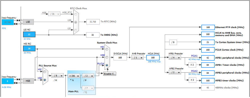
 In theory I have set all to the max speed with the clocking. APB1 is at 42 mhz (spis 2 and 3) and APB2 is 84mhz (SPI 1 ). This would make a 21 mbits spi for spi 2 & 3 and 42 mbits for spi 1, but instead as you can see in the other image I get 24mbits and 12mbits (It is not even a mult of the base frequency APB1/APB2)
#dma #discovery #spi #32f4
Hi
I have started a new project. I need to set 3xSPI at max speed. I'm using the discovery board with a STM32F407VGT6. This board has a 8mhz christal. I'm using cube, it is a nice tool that i'm starting to use with this project. I have configured the clocking setting in cube for this board to get the max speed possible in theory (check attached image and code) The initialization code is (only the dma/spi/clock functions are included):
void SystemClock_Config(void)
{
RCC_OscInitTypeDef RCC_OscInitStruct;
RCC_ClkInitTypeDef RCC_ClkInitStruct;
__PWR_CLK_ENABLE();
__HAL_PWR_VOLTAGESCALING_CONFIG(PWR_REGULATOR_VOLTAGE_SCALE1);
RCC_OscInitStruct.OscillatorType = RCC_OSCILLATORTYPE_LSI|RCC_OSCILLATORTYPE_HSE;
RCC_OscInitStruct.HSEState = RCC_HSE_ON;
RCC_OscInitStruct.LSIState = RCC_LSI_ON;
RCC_OscInitStruct.PLL.PLLState = RCC_PLL_ON;
RCC_OscInitStruct.PLL.PLLSource = RCC_PLLSOURCE_HSE;
RCC_OscInitStruct.PLL.PLLM = 8;
RCC_OscInitStruct.PLL.PLLN = 192;
RCC_OscInitStruct.PLL.PLLP = RCC_PLLP_DIV2;
RCC_OscInitStruct.PLL.PLLQ = 7;
HAL_RCC_OscConfig(&RCC_OscInitStruct);
RCC_ClkInitStruct.ClockType = RCC_CLOCKTYPE_SYSCLK|RCC_CLOCKTYPE_PCLK1
|RCC_CLOCKTYPE_PCLK2;
RCC_ClkInitStruct.SYSCLKSource = RCC_SYSCLKSOURCE_PLLCLK;
RCC_ClkInitStruct.AHBCLKDivider = RCC_SYSCLK_DIV1;
RCC_ClkInitStruct.APB1CLKDivider = RCC_HCLK_DIV4;
RCC_ClkInitStruct.APB2CLKDivider = RCC_HCLK_DIV2;
HAL_RCC_ClockConfig(&RCC_ClkInitStruct, FLASH_LATENCY_5);
}
void MX_SPI1_Init(void)
{
hspi1.Instance = SPI1;
hspi1.Init.Mode = SPI_MODE_MASTER;
hspi1.Init.Direction = SPI_DIRECTION_2LINES;
hspi1.Init.DataSize = SPI_DATASIZE_8BIT;
hspi1.Init.CLKPolarity = SPI_POLARITY_LOW;
hspi1.Init.CLKPhase = SPI_PHASE_1EDGE;
hspi1.Init.NSS = SPI_NSS_SOFT;
hspi1.Init.BaudRatePrescaler = SPI_BAUDRATEPRESCALER_2;
hspi1.Init.FirstBit = SPI_FIRSTBIT_LSB;
hspi1.Init.TIMode = SPI_TIMODE_DISABLED;
hspi1.Init.CRCCalculation = SPI_CRCCALCULATION_DISABLED;
HAL_SPI_Init(&hspi1);
}
/* SPI2 init function */
void MX_SPI2_Init(void)
{
hspi2.Instance = SPI2;
hspi2.Init.Mode = SPI_MODE_MASTER;
hspi2.Init.Direction = SPI_DIRECTION_2LINES;
hspi2.Init.DataSize = SPI_DATASIZE_8BIT;
hspi2.Init.CLKPolarity = SPI_POLARITY_LOW;
hspi2.Init.CLKPhase = SPI_PHASE_1EDGE;
hspi2.Init.NSS = SPI_NSS_SOFT;
hspi2.Init.BaudRatePrescaler = SPI_BAUDRATEPRESCALER_2;
hspi2.Init.FirstBit = SPI_FIRSTBIT_LSB;
hspi2.Init.TIMode = SPI_TIMODE_DISABLED;
hspi2.Init.CRCCalculation = SPI_CRCCALCULATION_DISABLED;
HAL_SPI_Init(&hspi2);
}
/* SPI3 init function */
void MX_SPI3_Init(void)
{
hspi3.Instance = SPI3;
hspi3.Init.Mode = SPI_MODE_MASTER;
hspi3.Init.Direction = SPI_DIRECTION_2LINES;
hspi3.Init.DataSize = SPI_DATASIZE_8BIT;
hspi3.Init.CLKPolarity = SPI_POLARITY_LOW;
hspi3.Init.CLKPhase = SPI_PHASE_1EDGE;
hspi3.Init.NSS = SPI_NSS_SOFT;
hspi3.Init.BaudRatePrescaler = SPI_BAUDRATEPRESCALER_2;
hspi3.Init.FirstBit = SPI_FIRSTBIT_LSB;
hspi3.Init.TIMode = SPI_TIMODE_DISABLED;
hspi3.Init.CRCCalculation = SPI_CRCCALCULATION_DISABLED;
HAL_SPI_Init(&hspi3);
}
void MX_DMA_Init(void)
{
/* DMA controller clock enable */
__DMA1_CLK_ENABLE();
__DMA2_CLK_ENABLE();
/* DMA interrupt init */
HAL_NVIC_SetPriority(DMA1_Stream4_IRQn, 0, 0);
HAL_NVIC_EnableIRQ(DMA1_Stream4_IRQn);
HAL_NVIC_SetPriority(DMA2_Stream3_IRQn, 0, 0);
HAL_NVIC_EnableIRQ(DMA2_Stream3_IRQn);
HAL_NVIC_SetPriority(DMA1_Stream5_IRQn, 0, 0);
HAL_NVIC_EnableIRQ(DMA1_Stream5_IRQn);
}
void HAL_SPI_MspInit(SPI_HandleTypeDef* hspi)
{
GPIO_InitTypeDef GPIO_InitStruct;
if(hspi->Instance==SPI1)
{
/* USER CODE BEGIN SPI1_MspInit 0 */
/* USER CODE END SPI1_MspInit 0 */
/* Peripheral clock enable */
__SPI1_CLK_ENABLE();
/**SPI1 GPIO Configuration
PA5 ------> SPI1_SCK
PA6 ------> SPI1_MISO
PA7 ------> SPI1_MOSI
*/
GPIO_InitStruct.Pin = GPIO_PIN_5|GPIO_PIN_6|GPIO_PIN_7;
GPIO_InitStruct.Mode = GPIO_MODE_AF_PP;
GPIO_InitStruct.Pull = GPIO_NOPULL;
GPIO_InitStruct.Speed = GPIO_SPEED_HIGH;
GPIO_InitStruct.Alternate = GPIO_AF5_SPI1;
HAL_GPIO_Init(GPIOA, &GPIO_InitStruct);
/* Peripheral DMA init*/
hdma_spi1_tx.Instance = DMA2_Stream3;
hdma_spi1_tx.Init.Channel = DMA_CHANNEL_3;
hdma_spi1_tx.Init.Direction = DMA_MEMORY_TO_PERIPH;
hdma_spi1_tx.Init.PeriphInc = DMA_PINC_DISABLE;
hdma_spi1_tx.Init.MemInc = DMA_MINC_ENABLE;
hdma_spi1_tx.Init.PeriphDataAlignment = DMA_PDATAALIGN_BYTE;
hdma_spi1_tx.Init.MemDataAlignment = DMA_MDATAALIGN_BYTE;
hdma_spi1_tx.Init.Mode = DMA_NORMAL;
hdma_spi1_tx.Init.Priority = DMA_PRIORITY_VERY_HIGH;
hdma_spi1_tx.Init.FIFOMode = DMA_FIFOMODE_DISABLE;
HAL_DMA_Init(&hdma_spi1_tx);
__HAL_LINKDMA(hspi,hdmatx,hdma_spi1_tx);
/* USER CODE BEGIN SPI1_MspInit 1 */
/* USER CODE END SPI1_MspInit 1 */
}
else if(hspi->Instance==SPI2)
{
/* USER CODE BEGIN SPI2_MspInit 0 */
/* USER CODE END SPI2_MspInit 0 */
/* Peripheral clock enable */
__SPI2_CLK_ENABLE();
/**SPI2 GPIO Configuration
PC2 ------> SPI2_MISO
PC3 ------> SPI2_MOSI
PB13 ------> SPI2_SCK
*/
GPIO_InitStruct.Pin = GPIO_PIN_2|GPIO_PIN_3;
GPIO_InitStruct.Mode = GPIO_MODE_AF_PP;
GPIO_InitStruct.Pull = GPIO_NOPULL;
GPIO_InitStruct.Speed = GPIO_SPEED_HIGH;
GPIO_InitStruct.Alternate = GPIO_AF5_SPI2;
HAL_GPIO_Init(GPIOC, &GPIO_InitStruct);
GPIO_InitStruct.Pin = GPIO_PIN_13;
GPIO_InitStruct.Mode = GPIO_MODE_AF_PP;
GPIO_InitStruct.Pull = GPIO_NOPULL;
GPIO_InitStruct.Speed = GPIO_SPEED_HIGH;
GPIO_InitStruct.Alternate = GPIO_AF5_SPI2;
HAL_GPIO_Init(GPIOB, &GPIO_InitStruct);
/* Peripheral DMA init*/
hdma_spi2_tx.Instance = DMA1_Stream4;
hdma_spi2_tx.Init.Channel = DMA_CHANNEL_0;
hdma_spi2_tx.Init.Direction = DMA_MEMORY_TO_PERIPH;
hdma_spi2_tx.Init.PeriphInc = DMA_PINC_DISABLE;
hdma_spi2_tx.Init.MemInc = DMA_MINC_ENABLE;
hdma_spi2_tx.Init.PeriphDataAlignment = DMA_PDATAALIGN_BYTE;
hdma_spi2_tx.Init.MemDataAlignment = DMA_MDATAALIGN_BYTE;
hdma_spi2_tx.Init.Mode = DMA_NORMAL;
hdma_spi2_tx.Init.Priority = DMA_PRIORITY_VERY_HIGH;
hdma_spi2_tx.Init.FIFOMode = DMA_FIFOMODE_DISABLE;
HAL_DMA_Init(&hdma_spi2_tx);
__HAL_LINKDMA(hspi,hdmatx,hdma_spi2_tx);
/* USER CODE BEGIN SPI2_MspInit 1 */
/* USER CODE END SPI2_MspInit 1 */
}
else if(hspi->Instance==SPI3)
{
/* USER CODE BEGIN SPI3_MspInit 0 */
/* USER CODE END SPI3_MspInit 0 */
/* Peripheral clock enable */
__SPI3_CLK_ENABLE();
/**SPI3 GPIO Configuration
PC10 ------> SPI3_SCK
PC11 ------> SPI3_MISO
PC12 ------> SPI3_MOSI
*/
GPIO_InitStruct.Pin = GPIO_PIN_10|GPIO_PIN_11|GPIO_PIN_12;
GPIO_InitStruct.Mode = GPIO_MODE_AF_PP;
GPIO_InitStruct.Pull = GPIO_NOPULL;
GPIO_InitStruct.Speed = GPIO_SPEED_HIGH;
GPIO_InitStruct.Alternate = GPIO_AF6_SPI3;
HAL_GPIO_Init(GPIOC, &GPIO_InitStruct);
/* Peripheral DMA init*/
hdma_spi3_tx.Instance = DMA1_Stream5;
hdma_spi3_tx.Init.Channel = DMA_CHANNEL_0;
hdma_spi3_tx.Init.Direction = DMA_MEMORY_TO_PERIPH;
hdma_spi3_tx.Init.PeriphInc = DMA_PINC_DISABLE;
hdma_spi3_tx.Init.MemInc = DMA_MINC_ENABLE;
hdma_spi3_tx.Init.PeriphDataAlignment = DMA_PDATAALIGN_BYTE;
hdma_spi3_tx.Init.MemDataAlignment = DMA_MDATAALIGN_BYTE;
hdma_spi3_tx.Init.Mode = DMA_NORMAL;
hdma_spi3_tx.Init.Priority = DMA_PRIORITY_VERY_HIGH;
hdma_spi3_tx.Init.FIFOMode = DMA_FIFOMODE_DISABLE;
HAL_DMA_Init(&hdma_spi3_tx);
__HAL_LINKDMA(hspi,hdmatx,hdma_spi3_tx);
/* USER CODE BEGIN SPI3_MspInit 1 */
/* USER CODE END SPI3_MspInit 1 */
}
}
int main(void)
{
/* USER CODE BEGIN 1 */
/* USER CODE END 1 */
/* MCU Configuration----------------------------------------------------------*/
/* Reset of all peripherals, Initializes the Flash interface and the Systick. */
HAL_Init();
/* Configure the system clock */
SystemClock_Config();
/* Initialize all configured peripherals */
MX_GPIO_Init();
MX_DMA_Init();
MX_IWDG_Init();
MX_SPI1_Init();
MX_SPI2_Init();
MX_SPI3_Init();
MX_TIM2_Init();
MX_TIM3_Init();
MX_TIM4_Init();
MX_TIM5_Init();
MX_TIM9_Init();
/* USER CODE BEGIN 2 */
/* USER CODE END 2 */
/* Infinite loop */
/* USER CODE BEGIN WHILE */
while (1)
{
/* USER CODE END WHILE */
/* USER CODE BEGIN 3 */
// Led On
HAL_GPIO_WritePin(GPIOD, GPIO_PIN_15, GPIO_PIN_SET);
if(HAL_SPI_Transmit_DMA(&hspi1, (uint8_t*)aTxBuffer, strlen((const char *) aTxBuffer)) != HAL_OK)
Error_Handler();
if(HAL_SPI_Transmit_DMA(&hspi2, (uint8_t*)aTxBuffer, strlen((const char *) aTxBuffer)) != HAL_OK)
Error_Handler();
if(HAL_SPI_Transmit_DMA(&hspi3, (uint8_t*)aTxBuffer, strlen((const char *) aTxBuffer)) != HAL_OK)
Error_Handler();
// Pause
//Soft_Delay(0x000FFFFF);
// Led Off
HAL_GPIO_WritePin(GPIOD, GPIO_PIN_15,GPIO_PIN_RESET);
// Pause
Soft_Delay(0x000FFFFF);
}
/* USER CODE END 3 */
} In theory I have set all to the max speed with the clocking. APB1 is at 42 mhz (spis 2 and 3) and APB2 is 84mhz (SPI 1 ). This would make a 21 mbits spi for spi 2 & 3 and 42 mbits for spi 1, but instead as you can see in the other image I get 24mbits and 12mbits (It is not even a mult of the base frequency APB1/APB2)
#dma #discovery #spi #32f4
Labels:
- Labels:
-
DMA
-
SPI
-
STM32F4 Series
2 REPLIES 2
Options
- Mark as New
- Bookmark
- Subscribe
- Mute
- Subscribe to RSS Feed
- Permalink
- Email to a Friend
- Report Inappropriate Content
2015-05-04 03:42 AM
Posted on May 04, 2015 at 12:42I have added some UARTs port at 115200 and they are working at right speed, so APB1 and APB2 speeds are in theory ok.Why do I get the SPIS at 1/2 of the speed then if all is configured right?
Options
- Mark as New
- Bookmark
- Subscribe
- Mute
- Subscribe to RSS Feed
- Permalink
- Email to a Friend
- Report Inappropriate Content
2015-05-06 01:01 AM
Posted on May 06, 2015 at 10:01
Any tip on this?. I have been searching with no luck. Spis are half of the max theorical speed, and only rising the apb1/apb2 to 2x the max speed I get the 42mbits/21mbits.
EDITED: Strange, I didnt change anything in clocking, or spis, just continued with other stuff (nothing with spis) but it is working now and i dont know why.... I would think that it is a cube bug but initialization was ok and it is the same that i have actually ...,
Related Content
- Error in sending message with FDCAN on STM32H735G-DK in STM32CubeIDE (MCUs)
- On Block Diagram which BUS connects to the RCC in STM32 MCUs Boards and hardware tools
- I don't know what I can do after full chip erase in STM32 MCUs Boards and hardware tools
- STM32F407 discovery card debug error, Core is held in reset in STM32 MCUs products
- stm32F412.. disco -- Unable to get the sdcard working. in STM32 MCUs products