- STMicroelectronics Community
- STM32 MCUs
- STM32 MCUs products
- STM32L47x ADC maximum input voltage
- Subscribe to RSS Feed
- Mark Topic as New
- Mark Topic as Read
- Float this Topic for Current User
- Bookmark
- Subscribe
- Mute
- Printer Friendly Page
STM32L47x ADC maximum input voltage
- Mark as New
- Bookmark
- Subscribe
- Mute
- Subscribe to RSS Feed
- Permalink
- Email to a Friend
- Report Inappropriate Content
2017-04-25 11:40 PM
Dear all,
I have the following situation:
- STM32L471/L476 processor
- Using the ADC with the internal reference buffer (2.5V) as analog eference
- One of the ADC input signals comes from a rail-to-rail OP-AMP with 3V supply voltage, so this input signal can be up to 3V, and therefore higher than the ADC reference voltage
- Normally this ADC input signal will be within 0 to 2.5V but it might occassionally exceed that range and then go up to 3V
Now my question is:
Is it a problem when the ADC input voltage is above the reference voltage? I know that some ADC's can get damaged in this case. In the datasheet I found that
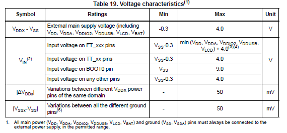
- GPIO VIN max = 4V (STM32L476xx Datasheet, DocID025976 Rev 3, Table 18)
- This absolute maximum rating I would fulfill
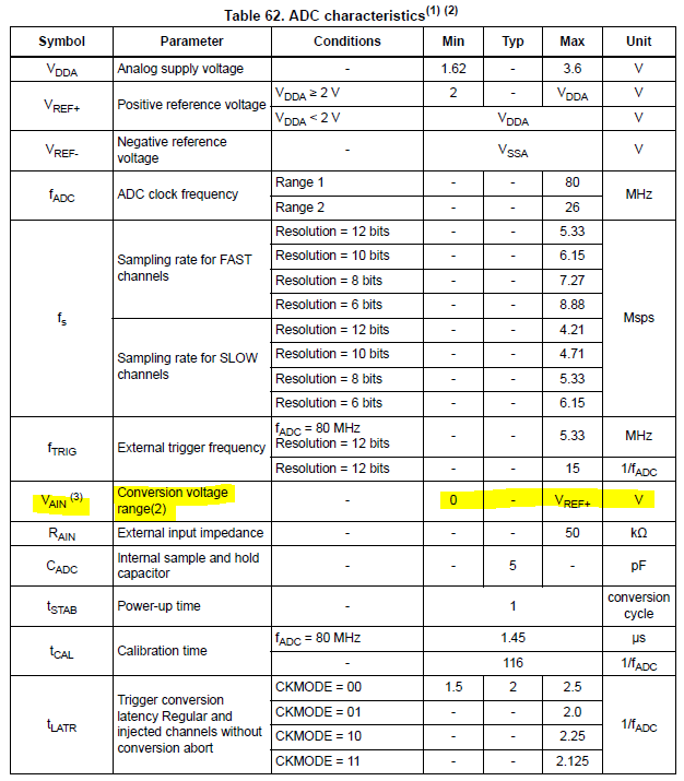
- ADC VAIN Conversion voltage range max = VREF+ (STM32L476xx Datasheet, DocID025976 Rev 3, Table 62)
- This looks like it is just where the ADC converts but not like a do-not-exceed limit
So if the ADC in this configuration can get damaged by a 3V voltage I would look for some alternative (other reference, limit input signal externally) but it would be the best if it could withstand it.
Additional information:
- I cannot use the 3V supply of the OP-AMPs as it is switched on/off but I need a constant analog refernce since I require the DACs all the time
- Using another 3V supply would be possible but costly (this is a device prototype)
Hope you could undestand my problem, otherwise just let me know.
Thanks in advance and kind regards
Markus
#stm32l4 #analog-inputs-for-adc- Labels:
-
STM32L4 Series
- Mark as New
- Bookmark
- Subscribe
- Mute
- Subscribe to RSS Feed
- Permalink
- Email to a Friend
- Report Inappropriate Content
2017-04-26 01:14 AM
As a general rule, being above the normal max operating means accelerated ageing before permanent damage.
Above AMR (Absolute Max Rating), the chip may be damaged anytime.
At AMR, the chip may be operational up to a certain time (typically 1000 hours?)
In between...
- Mark as New
- Bookmark
- Subscribe
- Mute
- Subscribe to RSS Feed
- Permalink
- Email to a Friend
- Report Inappropriate Content
2017-04-26 02:04 AM
I don't have a L47x board in my collection, which is already too large. So I didn't read the datasheet / reference manual for your specific part.
But I bet it (the datasheet) defines the maximal input voltage of the ADC, and supposedly identical to the maximal supply voltage (3.6V on other parts).
Quite sure there is no harm done in your case, but your ADC readbacks will be meaningless when above Vref.
If you can set Vref equal to Vcc as well, a supposed damage would be illogical.
- Mark as New
- Bookmark
- Subscribe
- Mute
- Subscribe to RSS Feed
- Permalink
- Email to a Friend
- Report Inappropriate Content
2017-04-27 02:26 AM
Unfortunately I could not find a maximal input voltage for the ADC in the datasheet. There is a limit for V_AIN, but it is described as ''Conversion voltage range'', see following picture from the datasheet. That the conversion voltage range spans from 0 to VREF+ is obvious but still leaves the question for maximum ADC input voltage.

I also would not expect harm but I hoped to get some definite answer on it.
Do you by chance know if an input-voltage-limit is defined for another ST-processor's ADC? Maybe that's a point to start from as I would expect ST to use similar ADC circuitries in different processors.
Thanks already for your quick reply and kind regards
Markus
- Mark as New
- Bookmark
- Subscribe
- Mute
- Subscribe to RSS Feed
- Permalink
- Email to a Friend
- Report Inappropriate Content
2017-04-27 03:11 AM
From the STM34L476 datasheet chapter 6.2 Absolute maximum ratings below:

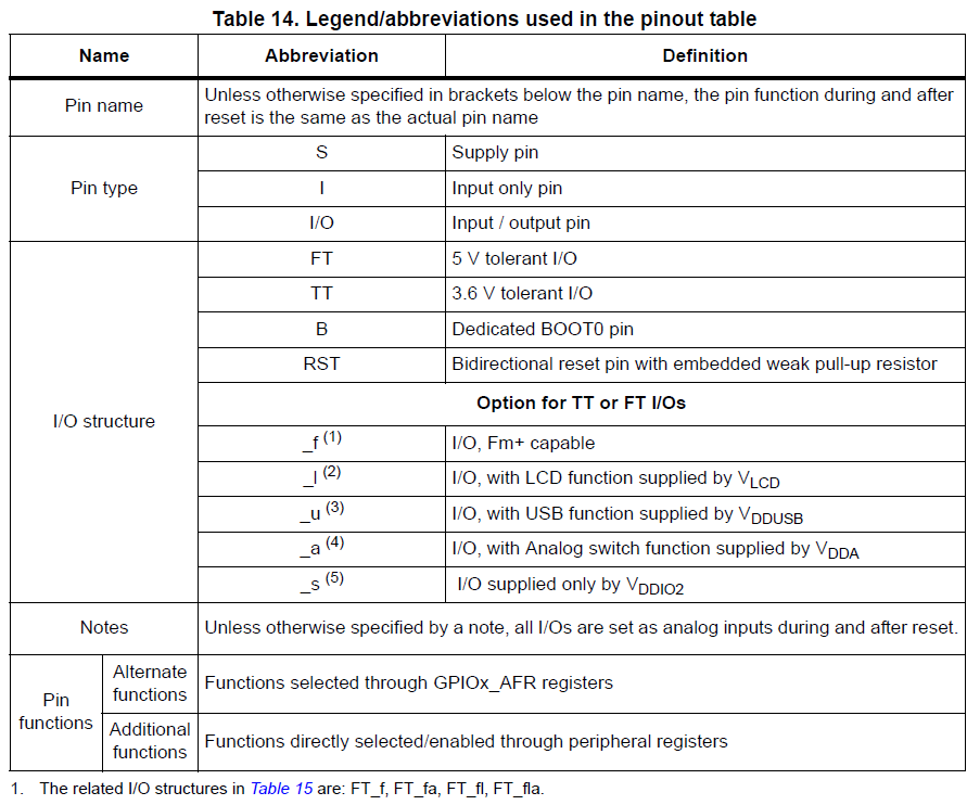
All STM32s have GPIO FT and FF type. This corresponds to the maximum and minimum guaranteed values.
- FT stands for 5 Volt Tolerant GPIO.
- FF stands for 3.6V Tolerant GPIO.
Generally Analog IO are FF_a or FT_a and Non-Analog IO are FT, I suggest you consult the datasheet of your device (chapter 4 )

In your case, I think there is no risk of destruction for the analog input and the ADC as long as your signal is less than 3.6V.
On the other hand if your VRef + is the internal reference 2.5V you will not be able to convert the variations of the input signal from 2.5V to 3.6V, there will be saturation of the conversion result.Change VRef to 3.3 (VDDA) or make a conditioning of your input signal by scaling to meet the full scale of your ADC.
To give better visibility on the answered topics, please click on Accept as Solution on the reply which solved your issue or answered your question.
- Mark as New
- Bookmark
- Subscribe
- Mute
- Subscribe to RSS Feed
- Permalink
- Email to a Friend
- Report Inappropriate Content
2017-04-27 03:15 AM
I also would not expect harm but I hoped to get some definite answer on it.
I interpret the parameter name 'Conversion voltage range' and the specified max. values (sect. 6.2, absolute maximum ratings) as definitive answer.
Do you by chance know if an input-voltage-limit is defined for another ST-processor's ADC? Maybe that's a point to start from as I would expect ST to use similar ADC circuitries in different processors.
The L devices seem to be reworked for low power, not sure about the protective circuitry. The datasheet for the L device you mention specifies 4.0 V for those analog inputs (TT_xx).
The limits used to be (Vdda + 0.3V) for pins connected to analog peripherals, like ADC inputs. Specifically checked with the F40x.
The term 'Conversion voltage range' means the voltage range that is converted to a proper binary representation.
'Not being converted properly' not automatically implies physical damage to the ADC, but it is probably an issue for your application.
- Mark as New
- Bookmark
- Subscribe
- Mute
- Subscribe to RSS Feed
- Permalink
- Email to a Friend
- Report Inappropriate Content
2017-05-04 10:10 AM
I confirm that there is no risk to damage the product in the case you are describing above.
- Mark as New
- Bookmark
- Subscribe
- Mute
- Subscribe to RSS Feed
- Permalink
- Email to a Friend
- Report Inappropriate Content
2017-05-09 05:02 AM
Ok, perfect!!!
Thank you everybody for your help, really appreciate it
- STM32C0 with 5V power as in AN392 in STM32 MCUs products
- STSPIN32G4 with a brushless drone motor in STM32 MCUs Motor control
- How to get printf() to write to USART2? Using NUCLEO-F401RE and IAR. in STM32 MCUs Embedded software
- VREF+ exceeding VDDA during power on/off in STM32 MCUs products
- Watchdog not wakeup from the STOP mode occasionally in STM32 MCUs products