- STMicroelectronics Community
- STM32 MCUs
- STM32 MCUs products
- STM32F429 PWM with Timer 2
- Subscribe to RSS Feed
- Mark Topic as New
- Mark Topic as Read
- Float this Topic for Current User
- Bookmark
- Subscribe
- Mute
- Printer Friendly Page
STM32F429 PWM with Timer 2
- Mark as New
- Bookmark
- Subscribe
- Mute
- Subscribe to RSS Feed
- Permalink
- Email to a Friend
- Report Inappropriate Content
2017-08-02 10:41 AM
I am using STM32F429 discovery board.
I am trying to generate pwm output on pin 11 of GPIO G. I have set and enabled the corresponding registers and bits but there is no output on pin 11. If I write a simple delay code then pin 11 does go high and the code works fine. I am coding using direct registers. Any suggestions?
&sharpinclude <stm32f4xx.h>
void clk_sys(){ RCC ->CFGR |= RCC_CFGR_MCO1_0; RCC ->CFGR |= RCC_CFGR_MCO1_1; RCC ->CR |= RCC_CR_PLLON; RCC ->APB1ENR |= RCC_APB1ENR_TIM2EN;}void enable_gpio()//setting pin 11 of port g for AF1 which corresponds to timer 2.{ RCC ->AHB1ENR |= RCC_AHB1ENR_GPIOGEN; //Enables port G input output pins by setting the corresponding bit in advanced high performance bus 1 register. GPIOG ->MODER |= GPIO_MODER_MODER11_1; //Configures pin 11 for alternate function mode by setting the corresponding bit in the mode register GPIOG ->OTYPER &= ~(GPIO_OTYPER_OT_11); //Makes the output type as push-pull by resetting the corresponding bit in output type register. GPIOG ->OSPEEDR |= GPIO_OSPEEDER_OSPEEDR11_1;//Makes the output high speed. GPIOG ->PUPDR &= ~(GPIO_PUPDR_PUPDR11);//No pull up or pull down. GPIOG ->AFR[1] |= GPIO_AF1_TIM2; }void generate_pwm(){TIM2 ->CCMR1 |= TIM_CCMR1_OC1M_2;
TIM2 ->CCMR1 |= TIM_CCMR1_OC1M_1; TIM2 ->CCMR1 &= ~(TIM_CCMR1_OC1M_0); TIM2 ->CCMR1 |= TIM_CCMR1_OC1PE; TIM2 ->CR1 |= TIM_CR1_ARPE; TIM2 ->EGR |= TIM_EGR_UG; TIM2 ->CCER |= TIM_CCER_CC1P; TIM2 ->CCER |= TIM_CCER_CC1E; TIM2 ->ARR = 0xFFF; TIM2 ->CCR1 = 0xFF; TIM2 ->CR1 |= TIM_CR1_CEN; HAL_TIM_PWM_Start; while(TIM2 ->CNT < TIM2 ->CCR1) { GPIOG ->BSRRL |= GPIO_BSRR_BS_11; }}int main(void){ clk_sys(); enable_gpio();while(1) { generate_pwm();// GPIOG ->BSRRL |= GPIO_BSRR_BS_11; }}#pwm #stm32fSolved! Go to Solution.
- Labels:
-
TIM
Accepted Solutions
- Mark as New
- Bookmark
- Subscribe
- Mute
- Subscribe to RSS Feed
- Permalink
- Email to a Friend
- Report Inappropriate Content
2017-08-02 01:48 PM
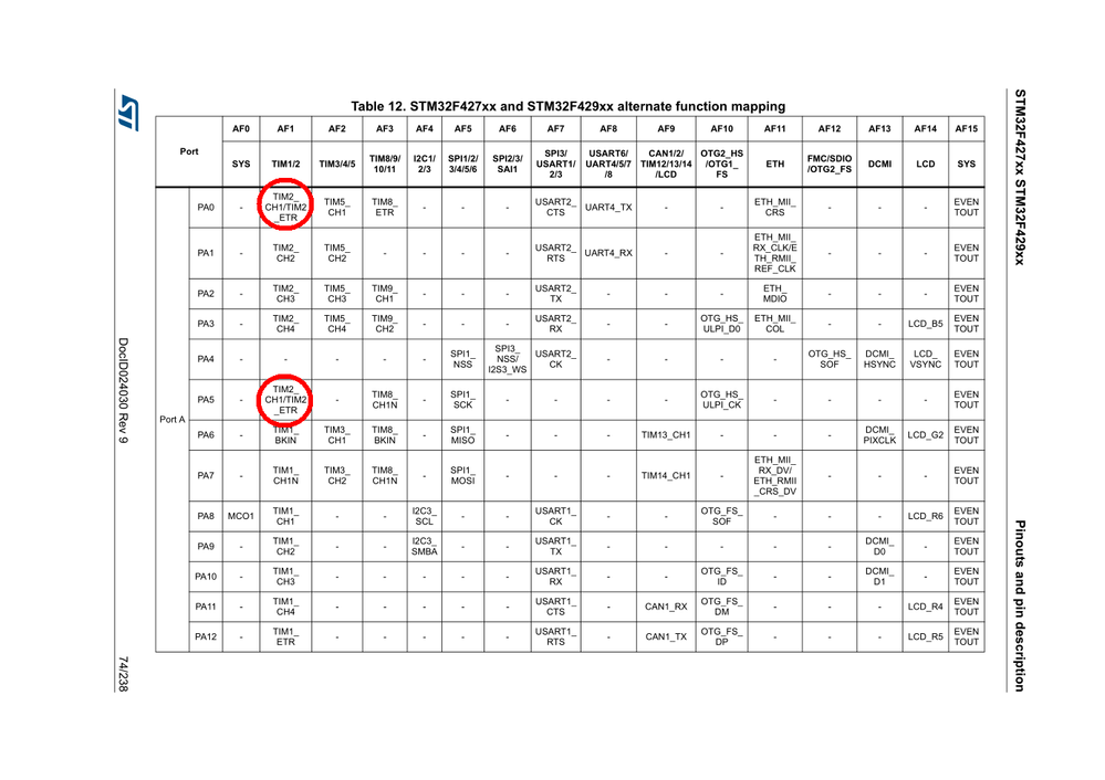
You can't assign functions to pins randomly. PG11 does not connect to TIM2_CH1 - for that you'd need PA0, PA5 or PA15. Look at the table in the STM32F429's datasheet:

etc.
GPIOG ->AFR[1] |= GPIO_AF1_TIM2;
This is probably wrong too. I don't know where do you have GPIO_AF1_TIM2 from, but most likely it's value is 1 and you'd need to shift it to left to match the pin's respective position in AFR[].
HAL_TIM_PWM_Start;
This is almost certainly not what you wanted. If you want to call a function, you must add the brackets, HAL_TIM_PWM_Start().
JW
- Mark as New
- Bookmark
- Subscribe
- Mute
- Subscribe to RSS Feed
- Permalink
- Email to a Friend
- Report Inappropriate Content
2017-08-02 01:48 PM
You can't assign functions to pins randomly. PG11 does not connect to TIM2_CH1 - for that you'd need PA0, PA5 or PA15. Look at the table in the STM32F429's datasheet:

etc.
GPIOG ->AFR[1] |= GPIO_AF1_TIM2;
This is probably wrong too. I don't know where do you have GPIO_AF1_TIM2 from, but most likely it's value is 1 and you'd need to shift it to left to match the pin's respective position in AFR[].
HAL_TIM_PWM_Start;
This is almost certainly not what you wanted. If you want to call a function, you must add the brackets, HAL_TIM_PWM_Start().
JW
- Mark as New
- Bookmark
- Subscribe
- Mute
- Subscribe to RSS Feed
- Permalink
- Email to a Friend
- Report Inappropriate Content
2017-08-03 08:11 AM
,
,
Thank you so much! I made the suggested changes. I had already found my mistake in taking pin G-11 and had replaced it with pin A5 already but all other suggestions helped a lot. The code is working fine now and I am getting desired output. For anyone who is having this problem, here is my updated code
♯ include <,stm32f4xx.h>,
,
void clk_sys(),
{,
RCC ->,CFGR |= RCC_CFGR_MCO1_0,,
RCC ->,CFGR |= RCC_CFGR_MCO1_1,,
RCC ->,CR |= RCC_CR_PLLON,,
RCC ->,APB1ENR |= RCC_APB1ENR_TIM2EN,,
},
void enable_gpio()//setting pin 11 of port g for AF1 which corresponds to timer 2.,
{,
RCC ->,AHB1ENR |= RCC_AHB1ENR_GPIOAEN, //Enables port G input output pins by setting the corresponding bit in advanced high performance bus 1 register.,
GPIOA ->,MODER |= GPIO_MODER_MODER5_1, //Configures pin 9 for alternate function mode by setting the corresponding bit in the mode register,
GPIOA ->,OTYPER &,= ~(GPIO_OTYPER_OT_5), //Makes the output type as push-pull by resetting the corresponding bit in output type register.,
GPIOA ->,OSPEEDR |= GPIO_OSPEEDER_OSPEEDR5_1,//Makes the output high speed.,
GPIOA ->,PUPDR &,= ~(GPIO_PUPDR_PUPDR5),//No pull up or pull down.,
GPIOA ->,AFR[0] = GPIO_AF1_TIM2<,<,20,,
},
void generate_pwm(),
{TIM2 ->,CCMR1 |= TIM_CCMR1_OC1M_2,
,
TIM2 ->,CCMR1 |= TIM_CCMR1_OC1M_1,,
TIM2 ->,CCMR1 &,= ~(TIM_CCMR1_OC1M_0),,
TIM2 ->,CCMR1 |= TIM_CCMR1_OC1PE,,
TIM2 ->,CR1 |= TIM_CR1_ARPE,,
TIM2 ->,EGR |= TIM_EGR_UG,,
TIM2 ->,CCER |= TIM_CCER_CC1P,,
TIM2 ->,CCER |= TIM_CCER_CC1E,,
TIM2 ->,ARR = 0x08,,
TIM2 ->,CCR1 = 0x06,,
TIM2 ->,CR1 |= TIM_CR1_CEN,while(TIM2 ->,CNT <, TIM2 ->,CCR1)
,
{,
GPIOA ->,BSRRL |= GPIO_BSRR_BS_5,,
},
},
int main(void),
{,
clk_sys(),,
enable_gpio(),,
while(1),
{,
generate_pwm(),,
// GPIOE ->,BSRRL |= GPIO_BSRR_BS_9,,
},
}- 8 pulse pin outputs on the STM32F407 (Drive GPIO with basic timer?) in STM32 MCUs products
- Multiple channels used for TIM1 in STM32 MCUs products
- I2C not working properly with sequencer. Why? in STM32 MCUs Wireless
- DAC-DMA and Timer in STM32CubeMX (MCUs)
- G431RBT6 - Interfacing timer and compare output timer have rather fluctuation timings in STM32 MCUs products