- STMicroelectronics Community
- STM32 MCUs
- STM32 MCUs products
- I2S ''R Division Factor''???
- Subscribe to RSS Feed
- Mark Topic as New
- Mark Topic as Read
- Float this Topic for Current User
- Bookmark
- Subscribe
- Mute
- Printer Friendly Page
I2S ''R Division Factor''???
- Mark as New
- Bookmark
- Subscribe
- Mute
- Subscribe to RSS Feed
- Permalink
- Email to a Friend
- Report Inappropriate Content
2017-09-25 01:12 PM
Hi - I'm trying to configure my STM32F429 Discovery board to send digital audio data to a
http://store.digilentinc.com/pmod-i2s-stereo-audio-output/
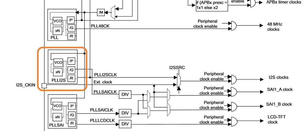
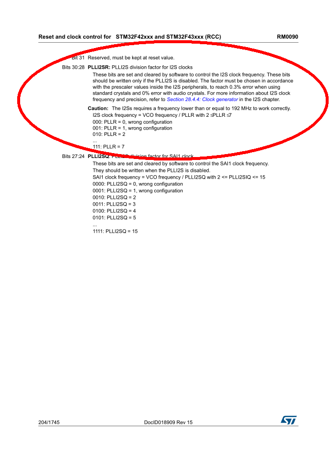
. Section 28.4.4 (pg 911) of the says:To achieve high-quality audio performance, the I2SxCLK clock source can be either the PLLI2S output (through R division factor) or an external clock (mapped to I2S_CKIN pin).
I can't find any other mention (let alone an explanation) of what this 'R division factor' is. Does anyone know what this means?
-Terence
#stm32f4 #i2sSolved! Go to Solution.
- Labels:
-
I2S
-
STM32F4 Series
Accepted Solutions
- Mark as New
- Bookmark
- Subscribe
- Mute
- Subscribe to RSS Feed
- Permalink
- Email to a Friend
- Report Inappropriate Content
2017-09-25 01:25 PM
- Mark as New
- Bookmark
- Subscribe
- Mute
- Subscribe to RSS Feed
- Permalink
- Email to a Friend
- Report Inappropriate Content
2017-09-25 01:25 PM
JW
- Mark as New
- Bookmark
- Subscribe
- Mute
- Subscribe to RSS Feed
- Permalink
- Email to a Friend
- Report Inappropriate Content
2017-09-25 01:26 PM
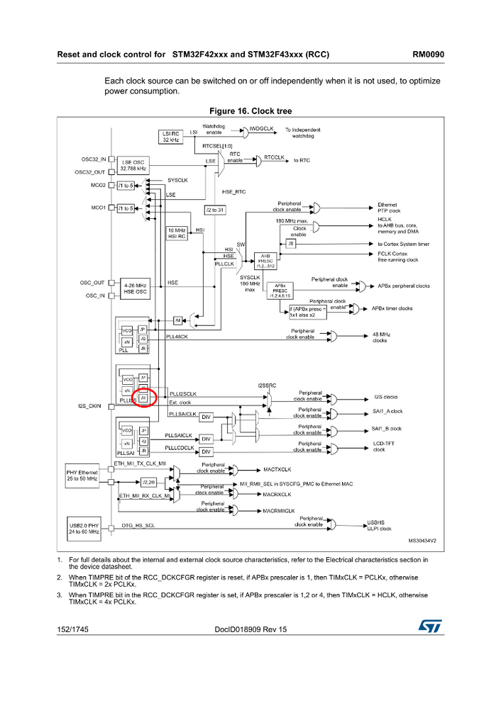
Each PLL has three divider taps for the VCO, P, Q and R. On the main one the P one goes to the processor, the Q to USB/SDIO.
Say you run the VCO at 360 MHz, a P setting of 2 gets you to 180 MHz.

- Mark as New
- Bookmark
- Subscribe
- Mute
- Subscribe to RSS Feed
- Permalink
- Email to a Friend
- Report Inappropriate Content
2017-09-25 03:46 PM
Ah, got it, thanks! Makes perfect sense after showing it to me on the clock tree diagram.
- Mark as New
- Bookmark
- Subscribe
- Mute
- Subscribe to RSS Feed
- Permalink
- Email to a Friend
- Report Inappropriate Content
2017-09-25 04:26 PM
Clive One wrote:
Each PLL has three divider taps for the VCO, P, Q and R. On the main one the P one goes to the processor, the Q to USB/SDIO.
Say you run the VCO at 360 MHz, a P setting of 2 gets you to 180 MHz.

Hi Clive - Follow up question to your example above just to make sure I'm understanding this properly: When you say ''Say you run the VCO at 360 MHz, a P setting of 2 gets you to 180 MHz'' this would be setting the PLLP bits of the RCC_PLLCFGR to zero and the PLLN bits of the same register to 101101000. Correct?
- Mark as New
- Bookmark
- Subscribe
- Mute
- Subscribe to RSS Feed
- Permalink
- Email to a Friend
- Report Inappropriate Content
2017-09-25 06:27 PM
- Mark as New
- Bookmark
- Subscribe
- Mute
- Subscribe to RSS Feed
- Permalink
- Email to a Friend
- Report Inappropriate Content
2017-09-25 07:25 PM
Clive One wrote:
Well presuming you use a 1 MHz comparison frequency, yes. For 2 MHz PLLN=180
Sorry, I'm new to this board. Searching the manual for 'comparison frequency' is not finding anything, nor do I see anything that rings a bell when looking through the RCC registers. Can you give me a hint on how this 1 or 2 MHz 'comparison frequency' is configured?
- Mark as New
- Bookmark
- Subscribe
- Mute
- Subscribe to RSS Feed
- Permalink
- Email to a Friend
- Report Inappropriate Content
2017-09-25 10:13 PM
Ok, so it's a PLL (Phase Locked Loop), you have a VCO (Voltage Controlled Oscillator, basically a very rapid pulse generator, whose frequency is controlled by an input voltage signal), you divide this down, by PLL_N, to a lower comparison frequency for the purpose of controlling the speed (for F4 this needs to be 1-2 MHz), and you take a reference clock, nominally HSE and divide that down by PLL_M to the same comparison frequency and you tune the VCO so as to match frequency and phase by controlling the VCO's voltage input.
ie HSE / PLL_M = VCO / PLL_N
So if HSE = 8 MHz, and PLL_M =8, then the comparison frequency will be 1 MHz, if PLL_M =4 then 2 MHz. In recent years ST seems to prefer the latter, but anywhere between 1 or 2 MHz is acceptable, and can be fractional if you have odd/unique clock sources. ie 16.368 MHz / 16 or 16.368 MHz / 15 or 19.2 MHz / 16
- Mark as New
- Bookmark
- Subscribe
- Mute
- Subscribe to RSS Feed
- Permalink
- Email to a Friend
- Report Inappropriate Content
2017-09-27 04:37 PM
Clive - Thanks for the additional explanation. One thing, you mention the following:
...you have a VCO (Voltage Controlled Oscillator, basically a very rapid pulse generator, whose frequency is controlled by an input voltage signal), you divide this down, by PLL_N...
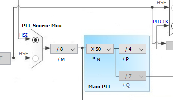
I'm not seeing this in in the clock configuration tool below - please see image below.

^It seems like it is not divided down by the PLL_N but instead divided down by the PLL_M and then multiplied by the PLL_N.
- Mark as New
- Bookmark
- Subscribe
- Mute
- Subscribe to RSS Feed
- Permalink
- Email to a Friend
- Report Inappropriate Content
2017-09-27 05:18 PM
That's because the 'xN' hides the nature of the PLL as Clive explained above: it's a VCO and its output frequency is divided down by N and (phase-)compared to the input frequency to PLL (which is the input frequency divided by M).
'Real' frequency multipliers are based on generating then filtering out harmonics. This is an entirely different process, with important consequences on output frequency stability/jitter/noise and vulnerability o being influenced externally eg. through power supply.
This is why the diagram from the RM is superior to that of CubeMX.
JW
- linux STM32CubeProgrammer fonts is too small in STM32CubeProgrammer (MCUs)
- STM32L4S5 Apparent discrepancy in maximum PLL clock in STM32 MCUs products
- Code generation - ADC3 prescaler in STM32CubeIDE (MCUs)
- Why does 'G0 ADC Calibration in Cube/HAL perform averaging in software? in STM32 MCUs products
- STM32WL5JC LoRa wireless transceiver Oscillator accuracy and stability in STM32 MCUs Wireless

