- STMicroelectronics Community
- STM32 MCUs
- STM32 MCUs products
- STM32F071V8 ADC ADC_IN17 (VREFINT) measurement err...
- Subscribe to RSS Feed
- Mark Topic as New
- Mark Topic as Read
- Float this Topic for Current User
- Bookmark
- Subscribe
- Mute
- Printer Friendly Page
STM32F071V8 ADC ADC_IN17 (VREFINT) measurement errors
- Mark as New
- Bookmark
- Subscribe
- Mute
- Subscribe to RSS Feed
- Permalink
- Email to a Friend
- Report Inappropriate Content
2018-02-14 05:33 AM
Hi all,
We are using a STM32F071V8 MCU in our project. I am polling the ADC to read the data and have followed the following procedure to initialize the ADC:
1. enable clock to respective GPIOs
2. Initialize GPIO pins as Analog Inputs3. Turn on HSI14MHZ clock
4. enable clock going to ADC5. reset ADC6. begin ADC calibration7. wait for calibration to finish 8. enable the ADC9. enable the VBAT divider and temperature sensor10. Configure the sampling time11. Configure ADC_CFGR1 register for settings - 12 bit resolution; Analog WDT disabled; Sinlge conversion mode 12. Configure ADC_CFGR2 register for settings - ADCCLK (Asynchronous clock mode)13. wait for ADC to finish starting upI was trying to determine the value of VDDA by using the formula below:
VDDA = 3.3 V x VREFINT_CAL / VREFINT_DATA
The
VREFINT_CAL value read is 1519. Upon reading the ADC_DR register after calibration I found the calibration factor to be 0x42.
When I poll for the data on the ADC_IN17 channel it varies drastically with respect to the sampling time.
Please find the results below:
SMP[2:0] = 000: 1.5 ADC clock cycles ; ADC counts = 1891; VDDA = 2.26V
001: 7.5 ADC clock cycles ; ADC counts = 1657; VDDA = 3.06V
010: 13.5 ADC clock cycles;
ADC counts = 1383; VDDA = 3.6V (Worse!)
011: 28.5 ADC clock cycles;
ADC counts = 1510; VDDA = 3.319V
Remains almost same for higher sampling time.
Could you please help me draw an inference here?
Thanks in advance.
#stm32f0-adc-vrefinit- Labels:
-
STM32F0 Series
- Mark as New
- Bookmark
- Subscribe
- Mute
- Subscribe to RSS Feed
- Permalink
- Email to a Friend
- Report Inappropriate Content
2018-02-14 06:10 AM
The data sheet mentions the minimum sampling time to read the Vrefinit as 4usec , so that explains the behavior probably.
- Mark as New
- Bookmark
- Subscribe
- Mute
- Subscribe to RSS Feed
- Permalink
- Email to a Friend
- Report Inappropriate Content
2018-02-14 06:44 PM
are you in a hurry ?
reduce the adc clock rate and don't use the fastest sampling rate..
it will settle down.
put a scope across Vdd/Vss look for your noise. looking from 20Mhz down to 10khz.
then similarly across Vdda / Vssa
then scope from Vssa to any analog input pin.
what bypassing do you have on the Vdda/Vssa pins ?
I use 1uF and 0.1uF on all Vdd/Vss pins.
- Mark as New
- Bookmark
- Subscribe
- Mute
- Subscribe to RSS Feed
- Permalink
- Email to a Friend
- Report Inappropriate Content
2018-02-15 12:24 AM
Hi TJ,
Thank you for the response. I will probe the Vdd/Vss for noise.
I need to sample the ADC data as quickly and efficiently I can. I have 0.1 and 10 uF caps on the Vdd/Vss pins.
- Mark as New
- Bookmark
- Subscribe
- Mute
- Subscribe to RSS Feed
- Permalink
- Email to a Friend
- Report Inappropriate Content
2018-02-15 01:11 AM
Pulling some things together:
9. enable the VBAT divider and temperature sensor
...
I need to sample the ADC data as quickly and efficiently I can.
Not sure if both statements belong together, but high sampling rates make no sense for this two parameters, as they are changing quite slow.
Even rates of one sample per second would be fine IMHO.
And don't forget to configure the sampling time according to your input impedances, else you get a 'drag effect', and increased noise.
- Mark as New
- Bookmark
- Subscribe
- Mute
- Subscribe to RSS Feed
- Permalink
- Email to a Friend
- Report Inappropriate Content
2018-02-15 08:03 AM
Hi AvaTar,
Thank you for the response. I am not using the VBAT and the temperature sensor in my code. I had configured them initially only to read the values.
When you say drag effect, are you conveying that the values may stabilize with time? Say for example the expected value is - 1519 what I would read would be something between 1410 - 1519?
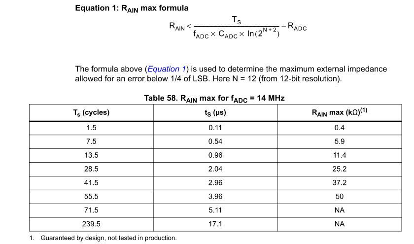
Also, the data sheet specifies the maximum external input impedance which is allowed. For sampling time of 5usec and above, the value of RAIN is referred as NA. Does it mean that the external input impedance does not matter for sampling time of 5usec and above?

- Mark as New
- Bookmark
- Subscribe
- Mute
- Subscribe to RSS Feed
- Permalink
- Email to a Friend
- Report Inappropriate Content
2018-02-15 09:05 AM
When you say drag effect, are you conveying that the values may stabilize with time
The source/input must be able to charge up the Sample&Hold capacitor in the given (sample) time, else you will see either a step-wise approximation of the actual value.
With multiple, multiplexed channels, the value seems 'dragged' towards the previously converted channel value.
The whole setup can easily approximated and calculated with a RC element (input impedance and S&H capacitor).
For sampling time of 5usec and above, the value of RAIN is referred as NA. Does it mean that the external input impedance does not matter for sampling time of 5usec and above?
I think they bravely omitted the calculation.
While 50kOhm is no problem for the most mediocre opamp, you cannot connect e.g. high-impedance sensors to the ADC inputs directly.
A noisy and/or unstable VDDA would account for large variance in ADC results.
VDDA should be buffered separately from VDD.
- Mark as New
- Bookmark
- Subscribe
- Mute
- Subscribe to RSS Feed
- Permalink
- Email to a Friend
- Report Inappropriate Content
2018-02-16 07:28 AM
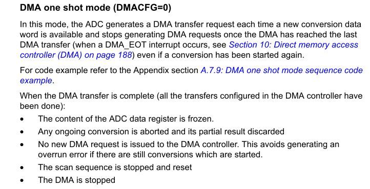
Thank you for the explanation. It was very helpful. I had an additional query. I am currently reading 6 analog channels using the DMA one shot mode. The DISCEN=0 and CONT= 0(I am sampling multiple channels in single conversion mode) .The data sheet says that, after the scan sequence the DMA is stopped. Does that mean that the DMAEN bit of the ADC_CFGR1 register becomes 0 or the EN bit of the DMA_CCR1 goes 0? However, I don't find any one of them go 0 in the watch window.
