- STMicroelectronics Community
- STM32 MCUs
- STM32 MCUs products
- DMA from internal SRAM to FMC missing first byte
- Subscribe to RSS Feed
- Mark Topic as New
- Mark Topic as Read
- Float this Topic for Current User
- Bookmark
- Subscribe
- Mute
- Printer Friendly Page
DMA from internal SRAM to FMC missing first byte
- Mark as New
- Bookmark
- Subscribe
- Mute
- Subscribe to RSS Feed
- Permalink
- Email to a Friend
- Report Inappropriate Content
2018-04-29 06:07 PM
I'm using a Nucleo -F722ZE to interface with an FPGA. The instruction and data cache are disabled. I have timer interrupts to set off the DMA at specific times with 128 bytes per transfer. No matter how I set up the DMA, the first byte is not transmitted. It is clear the DMA engine thinks it was because it terminates without error. I'm actually sending 50 blocks of 128 bytes, and there is a glitch transaction on the odd transfers where the first byte should be, but all the even transfers even that is not present.
I have tried byte to byte and word to byte transfers, as well as no burst and 16 or 4 burst. The timing is the same no matter what - I miss the first byte. Is there something I have to do to 'warm up' the FMC before the DMA gets turned on? I would prefer not to initiate a transfer because it would screw up the over all timing.
If anyone has any ideas, I'd love to hear them. I suppose I could try to send 129 bytes so I get 128, but that's just hoping the glitch doesn't get seen by the FPGA. It should just work.
Mike
#dma #fmc #sram Note: this post was migrated and contained many threaded conversations, some content may be missing.- Mark as New
- Bookmark
- Subscribe
- Mute
- Subscribe to RSS Feed
- Permalink
- Email to a Friend
- Report Inappropriate Content
2018-05-01 05:54 PM
I found a hack that works. In the timer interrupt which fires the DMA I first send 2 bytes out the FMC with the CPU. This does not show up on the FMC bus, but when the DMA fires, all 128 bytes appear. There is an address/data glitch before the DMA starts writing, but this has no write strobe so it is a don't care state.
for(i=0; i<2; i++) ptr[0] = image_buf[offset]; // dummy transmit
DMA2_Stream0->CR |= 1; // turn on DMA engine
Just sending 1 byte does not work. Sending more than 2 expands the time between the bus glitch and the first byte coming out the DMA.
I also found disabling the FMC FIFO made no difference, so I kept it enabled.
- Mark as New
- Bookmark
- Subscribe
- Mute
- Subscribe to RSS Feed
- Permalink
- Email to a Friend
- Report Inappropriate Content
2018-05-03 04:27 PM
This does not sound to be DMA-specific, once you see external bus cycles missing even at 'manual' write to FMC.
I guess this boils down to the particular FMC settings. You may want to read out and check/post the FMC registers, and perhaps also the GPIO registers of related pins. You don't fiddle with the GPIO settings of FMC pins, do you? You also may want to post the waveforms you've observed; perhaps constructing simplified examples still exhibiting the problem. How do you observe the pins, how did you see the 'glitch' - using a LA, or oscilloscope? Can't this be some sort of 'analog' problem?
JW
- Mark as New
- Bookmark
- Subscribe
- Mute
- Subscribe to RSS Feed
- Permalink
- Email to a Friend
- Report Inappropriate Content
2018-05-04 07:41 AM
Once I set the registers I don't touch them for the GPIO because I want the external bus to be permanent. If I let the CPU send data it comes in bursts of 2 or 3 bytes with a gap about 5 times the burst width. I'm using the LA portion of an MSO, and one of the things I was thinking of doing was looking at the analog portion. The first byte might be there but could be too small in time to capture. I don't think my FPGA would see it either though, it's internal clock is only 20 MHz.
I'll try to get some screen captures this weekend. I'm happy I've got a way to make it work but it'd be nice to know if I'm doing something stupid!
- Mark as New
- Bookmark
- Subscribe
- Mute
- Subscribe to RSS Feed
- Permalink
- Email to a Friend
- Report Inappropriate Content
2018-05-04 08:54 PM
Boy do I like modern 'scopes - capturing these images was trivial.
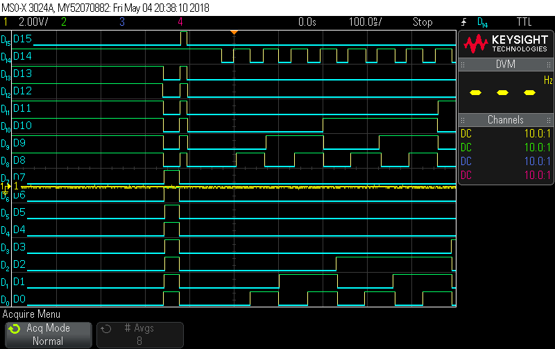
So here is what I first got with just DMA from internal RAM to FMC bus:

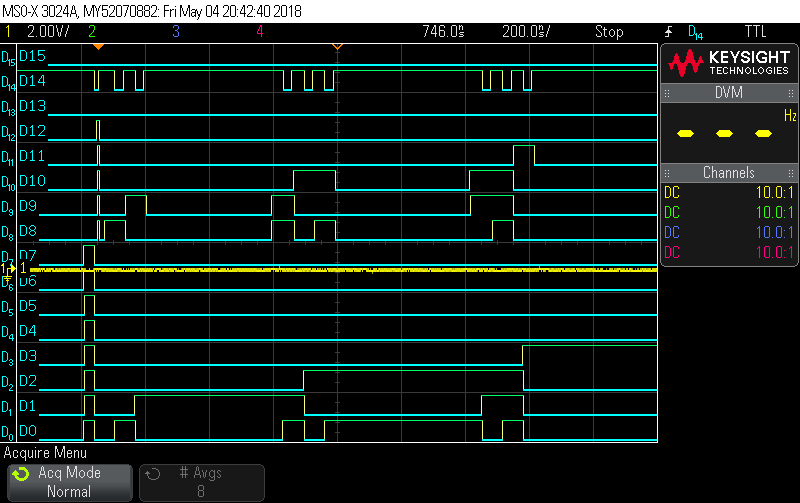
D0-D7 is data, I count from 0 to FF but split into two 128 byte blocks. D8-D13 is lower address, D14 is NWE and D15 is a GPIO signal for the FPGA. The ''glitch'' is on D8-D13 and D15 at the start of transfer. To see what was happening I removed the DMA and just used the CPU to write to the FMC. That resulted in this:

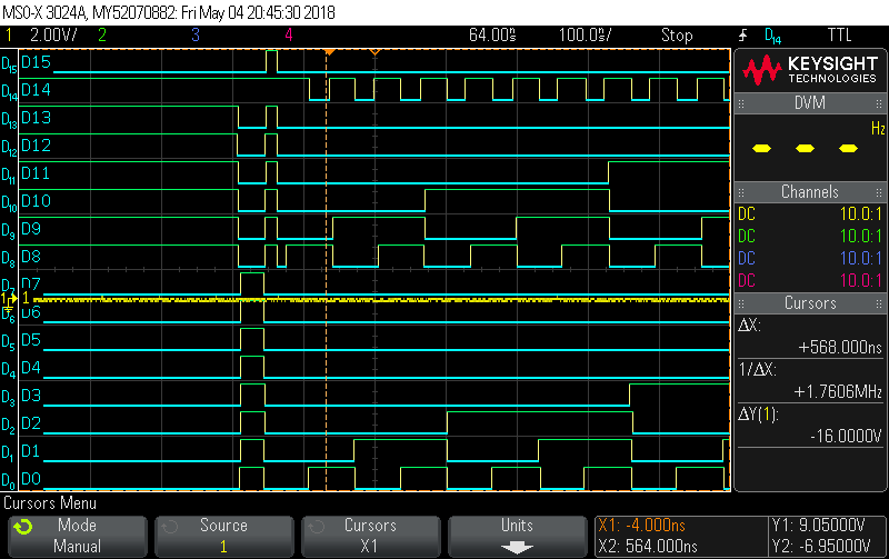
Cache is disabled for both instruction and data. Note that D15 does not glitch, but the other lines do. That might rule out cross talk (an analog problem) but maybe not. The first byte of 0 is still missing. So I then wrote 2 bytes using the CPU before firing the DMA and got it to work:

The glitch is still there, but the first DMA write is data byte 0 on address 0. The FPGA will use the address on falling edge of NWE and the data on rising edge, so this is perfect. My GPIO signal for the command is much wider so I can ignore the glitch on D15.
It's very curious why this happens this way. I can get what I need, and that's all that matters at this point!
- Mark as New
- Bookmark
- Subscribe
- Mute
- Subscribe to RSS Feed
- Permalink
- Email to a Friend
- Report Inappropriate Content
2018-05-06 09:07 AM
This all is unexpected.
I'd like to ask details on the 2nd picture ('manual write' - it's IMO better separate what appears to be a FMC problem from ). How exactly did you write? Are the bursts of 3 writes intended? What is before the first write - isn't there any write? Can you show code? Can you please read out the content of FMC and relevant GPIO registers and post it?
Also, did you use the analog function to observe the glitch, on whatever line (but certainly on the write(D15))? Can't this be some grounding issue? Can't there be some short which generates a glitch on the supply of the particular port? Can't there be some momentary conflict on the buses from the FPGA side (i.e. can't both the MCU and FPGA attempt to output data to the bus at the same time)?
JW
- Mark as New
- Bookmark
- Subscribe
- Mute
- Subscribe to RSS Feed
- Permalink
- Email to a Friend
- Report Inappropriate Content
2018-05-07 08:47 AM
Howdy JW,
I'll post the code this evening when I get back to the lab. It's really simple, and maybe that's part of the problem. I just set up the FMC using the GPIO registers, then use a pointer to read SRAM and write the FMC address.
It definitely could be a ground problem. I have two logic probes on one cable into the MSO and only 1 ground for each probe. The FPGA is not connected in these traces, I'm just toggling the lines directly into the scope. The FPGA isn't happy with the inputs yet, so that's another level of debugging. But it has nothing to do with the STM32. Also, it's a one way bus into the FPGA. The purpose of the D15 signal is to tell the FPGA to process the data. (It then forwards the data to other FPGA's each of which has a specific display task, so nothing needs to comes back.)
I didn't look with the analog probes to see what the signals really look like. It's possible the lines are just floating and that's why it looks like a glitch at first. But the lack of NWE for the first byte is real, so priming the FMC with CPU writes before turning on the DMA engine solves my problem. If that's weird, then it is likely I have the FMC set up wrong and it would be good to figure out what I did. So I'll post the code when I get a chance.
Mike
- Mark as New
- Bookmark
- Subscribe
- Mute
- Subscribe to RSS Feed
- Permalink
- Email to a Friend
- Report Inappropriate Content
2018-05-07 07:28 PM
- Mark as New
- Bookmark
- Subscribe
- Mute
- Subscribe to RSS Feed
- Permalink
- Email to a Friend
- Report Inappropriate Content
2018-05-08 03:09 AM
This all looks reasonable, except that you should set GPIO_OSPEEDR for the FMC pins to an adequate value to required output speed.
JW
PS. Can't the timer fire, i.e. the read happen, *before* the FMC has been set up?
- Mark as New
- Bookmark
- Subscribe
- Mute
- Subscribe to RSS Feed
- Permalink
- Email to a Friend
- Report Inappropriate Content
2018-05-08 07:52 AM
Thanks, I'll double check the OSPEEDR. It's only 5 to 10 MHZ, which these days is 'slow'.
I don't think the order matters. The FMC just has to be set up before I need it. Since it's done only once, I figure it's the first thing to do. Once the timer fires, the system is an infinite loop repeating 50 blocks of 128 bytes (with a spread of 340 usec between blocks) at 20 Hz. I could set up the timer first, but in terms of priority to the system I like putting hardware first.
Thanks for looking at it. It's always good to have someone else double check what I do!!!
Mike
- B-WL5M-SUBG1 Power consumption measurement in STM32 MCUs Wireless
- problem reading data from SCD30 with NUCLEO-L476RG in STM32 MCUs products
- STM32 Nucelo F429ZI, LWIP a simple application not working in STM32 MCUs products
- erase and write Internal flash in STM32CubeIDE (MCUs)
- Problems with Comparator/DAC on STM32G473 in STM32 MCUs products