- STMicroelectronics Community
- STM32 MCUs
- STM32 MCUs products
- Not able to read from an external EEPROM
- Subscribe to RSS Feed
- Mark Topic as New
- Mark Topic as Read
- Float this Topic for Current User
- Bookmark
- Subscribe
- Mute
- Printer Friendly Page
Not able to read from an external EEPROM
- Mark as New
- Bookmark
- Subscribe
- Mute
- Subscribe to RSS Feed
- Permalink
- Email to a Friend
- Report Inappropriate Content
2018-07-10 08:05 AM
I'm trying to write and read from an external
http://ww1.microchip.com/downloads/en/DeviceDoc/20001749K.pdf
. The datasheet states that I need to send an Enable code before I do anything. There is a start bit (SB) followed by an opcode, then a 6-bit address and then the actual data. I've combined the SB and opcode into one byte that I can send as a start condition. I'm able to enable, erase and then write to the EEPROM. I'm assuming this is working since the status returns HAL_OK and I can see the valid waveforms on the scope. What I can't seem to do is read the data back. For the READ operation I don't see any waveforms on the scope.Here is the main code:
int main(void)
{
 /* USER CODE BEGIN 1 */
 /* USER CODE END 1 */
 /* MCU Configuration----------------------------------------------------------*/
 /* Reset of all peripherals, Initializes the Flash interface and the Systick. */
 HAL_Init();
 /* USER CODE BEGIN Init */
 /* USER CODE END Init */
 /* Configure the system clock */
 SystemClock_Config();
 /* USER CODE BEGIN SysInit */
 /* USER CODE END SysInit */
 /* Initialize all configured peripherals */
 MX_GPIO_Init();
 MX_SPI1_Init();
 /* USER CODE BEGIN 2 */
 __HAL_SPI_ENABLE(&hspi1);
 /* USER CODE END 2 */
 /* Infinite loop */
 /* USER CODE BEGIN WHILE */

 HAL_GPIO_WritePin(CS_GPIO_Port, CS_Pin, GPIO_PIN_SET);
 HAL_Delay(10);
 enable_status = Enable_EEPROM(&EEPROM_SPI_PORT);
 HAL_Delay(10);
 erase_status = Erase_EEPROM(&EEPROM_SPI_PORT, addr);
 HAL_Delay(10);
 write_status = Write_EEPROM(&EEPROM_SPI_PORT, addr, tx_data);
 HAL_Delay(10);
 read_status = Read_EEPROM(&EEPROM_SPI_PORT, addr, rx_data);
 HAL_Delay(10);
 HAL_GPIO_WritePin(CS_GPIO_Port, CS_Pin, GPIO_PIN_RESET);
 while (1)
 {
 /* USER CODE END WHILE */
 /* USER CODE BEGIN
 }
 /* USER CODE END 3 */
}
�?�?�?�?�?�?�?�?�?�?�?�?�?�?�?�?�?�?�?�?�?�?�?�?�?�?�?�?�?�?�?�?�?�?�?�?�?�?�?�?�?�?�?�?�?�?�?�?�?�?�?�?�?�?�?�?�?
Here is the SPI initialization:
SPI_HandleTypeDef hspi1;
/* SPI1 init function */
void MX_SPI1_Init(void)
{
 hspi1.Instance = SPI1;
 hspi1.Init.Mode = SPI_MODE_MASTER;
 hspi1.Init.Direction = SPI_DIRECTION_2LINES;
 hspi1.Init.DataSize = SPI_DATASIZE_16BIT;
 hspi1.Init.CLKPolarity = SPI_POLARITY_LOW;
 hspi1.Init.CLKPhase = SPI_PHASE_1EDGE;
 hspi1.Init.NSS = SPI_NSS_SOFT;
 hspi1.Init.BaudRatePrescaler = SPI_BAUDRATEPRESCALER_64;
 hspi1.Init.FirstBit = SPI_FIRSTBIT_MSB;
 hspi1.Init.TIMode = SPI_TIMODE_DISABLE;
 hspi1.Init.CRCCalculation = SPI_CRCCALCULATION_DISABLE;
 hspi1.Init.CRCPolynomial = 10;
 if (HAL_SPI_Init(&hspi1) != HAL_OK)
 {
 _Error_Handler(__FILE__, __LINE__);
 }
}
�?�?�?�?�?�?�?�?�?�?�?�?�?�?�?�?�?�?�?�?�?�?�?�?
And here is how the Enable, Erase, Read and Write functions of the EEPROM are written.
#define ERASE0x07 // erase specific memory location. This is followed by the 8-bit address and then by the 16-bit data.
#define READ0x06 // read the memory location.
#define WRITE0x05 // write to the memory location
#define EEPROM_SPI_PORT hspi1
extern SPI_HandleTypeDef EEPROM_SPI_PORT;
uint8_t Enable_EEPROM (SPI_TypeDef *spi_handle) {
uint16_t ewen = (0x04 << 8) | 0b00110000;
if (HAL_SPI_Transmit(spi_handle, &ewen, 1, HAL_MAX_DELAY) == HAL_OK) return TRUE;
else return FALSE;
}
uint8_t Erase_EEPROM (SPI_TypeDef *spi_handle, uint8_t addr) {
uint16_t write_package;
write_package = (ERASE << 8 | addr);
if (HAL_SPI_Transmit(spi_handle, &write_package, 1, HAL_MAX_DELAY) == HAL_OK) return TRUE;
else return FALSE;
}
uint8_t Write_EEPROM (SPI_TypeDef *spi_handle, uint8_t addr, uint16_t data) {
uint16_t write_package[2];
write_package[0] = (WRITE << 8 | addr);
write_package[1] = data;
if (HAL_SPI_Transmit(spi_handle, write_package, 2, HAL_MAX_DELAY) == HAL_OK) return TRUE;
else return FALSE;
}
uint8_t Read_EEPROM (SPI_TypeDef *spi_handle, uint8_t addr, uint16_t data) {
uint16_t write_package;
write_package = (READ << 8 | addr);
if (HAL_SPI_TransmitReceive(spi_handle, &write_package, &data, 1, HAL_MAX_DELAY) == HAL_OK) return TRUE;
else return FALSE;
}
�?�?�?�?�?�?�?�?�?�?�?�?�?�?�?�?�?�?�?�?�?�?�?�?�?�?�?�?�?�?�?�?�?�?- Mark as New
- Bookmark
- Subscribe
- Mute
- Subscribe to RSS Feed
- Permalink
- Email to a Friend
- Report Inappropriate Content
2018-07-10 05:41 PM
I think you have the SPI nSS pin upside down...
HAL_GPIO_WritePin(CS_GPIO_Port, CS_Pin, GPIO_PIN_SET);// should drop nSS here... HAL_Delay(10); enable_status = Enable_EEPROM(&EEPROM_SPI_PORT); HAL_Delay(10); erase_status = Erase_EEPROM(&EEPROM_SPI_PORT, addr); HAL_Delay(10); write_status = Write_EEPROM(&EEPROM_SPI_PORT, addr, tx_data); HAL_Delay(10); read_status = Read_EEPROM(&EEPROM_SPI_PORT, addr, rx_data); HAL_Delay(10); HAL_GPIO_WritePin(CS_GPIO_Port, CS_Pin, GPIO_PIN_RESET);
//should raise nSS here...- Mark as New
- Bookmark
- Subscribe
- Mute
- Subscribe to RSS Feed
- Permalink
- Email to a Friend
- Report Inappropriate Content
2018-07-10 09:08 PM
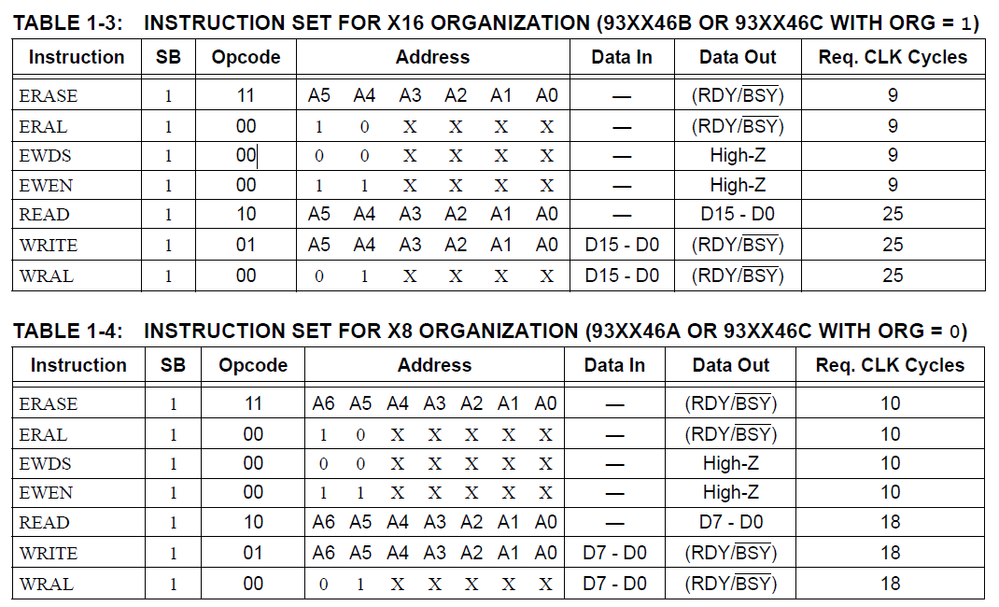
did you see this?
table 1-3 INSTRUCTION SET FOR X16 ORGANIZATION (93XX46B OR 93XX46C WITH ORG = 1)
how many clock cycles are you sending ?

- Mark as New
- Bookmark
- Subscribe
- Mute
- Subscribe to RSS Feed
- Permalink
- Email to a Friend
- Report Inappropriate Content
2018-07-10 09:28 PM
The chip's CS is active high. From the data sheet:
A high level selects the device; a low level deselects the device and forces it into Standby mode.
- Mark as New
- Bookmark
- Subscribe
- Mute
- Subscribe to RSS Feed
- Permalink
- Email to a Friend
- Report Inappropriate Content
2018-07-10 11:03 PM
that's so unusual,
did you see this note ?:
For added protection, an EWDS command should be performed after every write
operation and an external 10 k�?� pulldown protection resistor should be added to the CS pin.For the READ operation I don't see any waveforms on the scope.
can you see the clock cycle 16 times ?
is the function
Read_EEPROM - Mark as New
- Bookmark
- Subscribe
- Mute
- Subscribe to RSS Feed
- Permalink
- Email to a Friend
- Report Inappropriate Content
2018-07-10 11:53 PM
I missed seeing the note about EWDS and pulling the CS pin with a 10K resistor. I just tried that and it still can't seem to read. I see no clock cycles for the READ operation but I see that the function returned a TRUE which means it executed without any errors. Strange.
Also before using HAL_SPI_TransmitReceive, I tried sending the instruction for READ using just HAL_SPI_Transmit and then a tried to read from the EEPROM using HAL_SPI_Receive with a small delay between the two. That didn't work either.
Yes I saw this map and most of the addressing is based on this. I don't know how I can send odd number of clock cycles since all the data is either 8, 16 or 32-bit. Wherever there are 25 or 29 clock cycles need, I seem to be sending 32 and where the required cycles are 9, I seem to be sending 16.
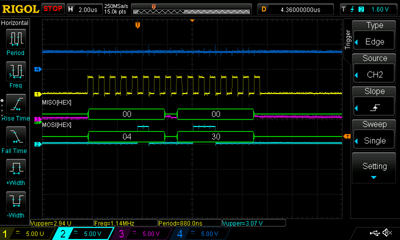
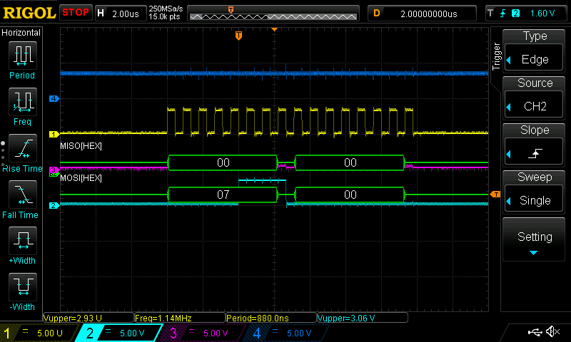
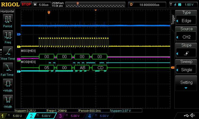
Here are the scope waveforms for ENABLE, ERASE and WRITE.
For ENABLE (Start bit is 1 and opcode for ENABLE is 00. Combining them comes to 0x04)

For ERASE (the 0x00 is the EEPROM address that I want to erase. Start bit is 1 and opcode for ERASE is 11. Combining them comes to 0x07).

For WRITE (address is 0x00, data is 0xABCD. Start bit is 1 and opcode for WRITE is 01. Combining them comes to 0x05).

- can Ewarm project be opened in Keil or CubeIDE ? in STM32 MCUs Boards and hardware tools
- STM32L4P5VGT - CDC, MSC and Pen Drive Support on USB in STM32 MCUs Embedded software
- STM32F412 I2C2 Busy flag keeps set in STM32 MCUs products
- Touchgfx base classes on external flash memory in STM32 MCUs TouchGFX and GUI
- Trigger from Timer does not trigger injected conversion on ADC in STM32 MCUs products