- STMicroelectronics Community
- Product forums
- Power management
- L6388E design support
- Subscribe to RSS Feed
- Mark Topic as New
- Mark Topic as Read
- Float this Topic for Current User
- Bookmark
- Subscribe
- Mute
- Printer Friendly Page
L6388E design support
- Mark as New
- Bookmark
- Subscribe
- Mute
- Subscribe to RSS Feed
- Permalink
- Email to a Friend
- Report Inappropriate Content
2018-06-27 06:21 AM
Hi all,
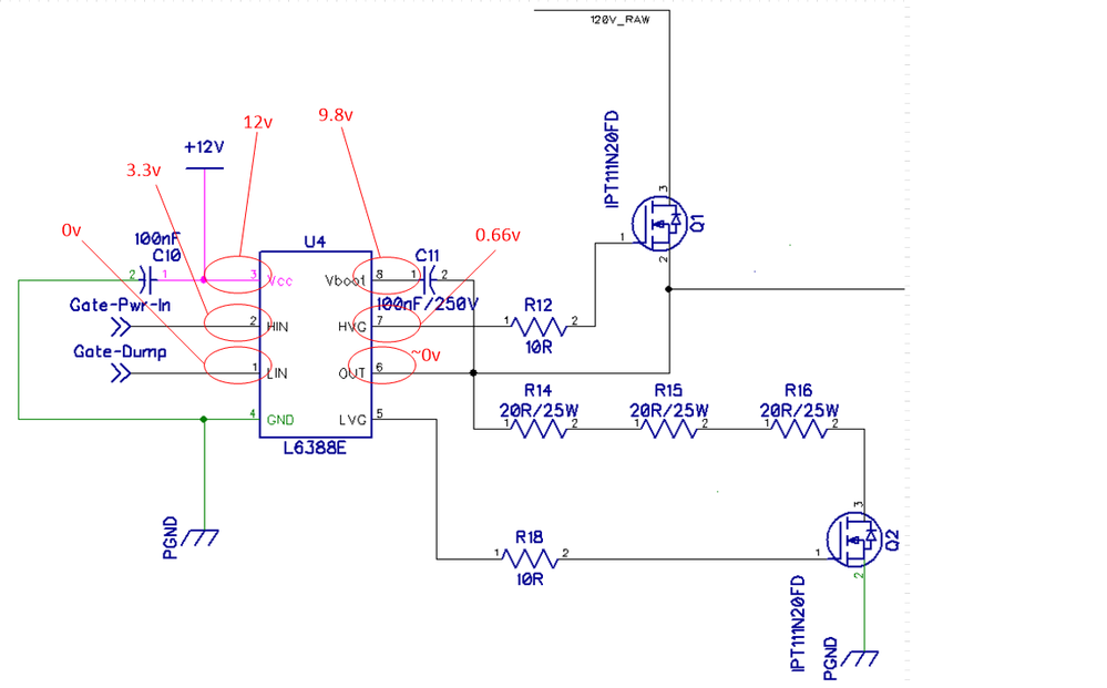
I'm in the process of bringing up a new design using the L6388E gate drivers. However, I've run into a stumbling block. Hopefully its something stupid in the design, but I'm at a loss: was wondering if anyone has any ideas?
I'm applying constant voltage to the HIN pin, but getting nout out on the gate line. All the other voltages are reading good, however. Cext calculations for these FETS come out at 8.3nF: so that 100nF bootstrap should be gross overkill. Voltage readings appended to the schematic below.
Any ideas?
Mat
- Labels:
-
Motor Control Hardware
- Mark as New
- Bookmark
- Subscribe
- Mute
- Subscribe to RSS Feed
- Permalink
- Email to a Friend
- Report Inappropriate Content
2018-06-27 11:56 PM
forum nobbled the original picture...

- Mark as New
- Bookmark
- Subscribe
- Mute
- Subscribe to RSS Feed
- Permalink
- Email to a Friend
- Report Inappropriate Content
2018-10-23 01:10 AM
A late reply but i could helpful to others.
HVG could not rise up for a simple reason:
HIN pin sensible to edges (while LIN is sensible to level) once VCC and VBO(VBOOT-OUT) are not in UVLO state (above UVLOthon).
In other words, it is first required first to supply VCC, turn on low side Q2 to charge the bootstrap capacitor C11 by rising LIN. Only once C11 is charged you can rise HVG by rising HIN. If you keep it static from the beginning HVG cannot rise up.
Moreover L6388 have interlocking, to protect most application topologies, you cannot rise LVG and HVG simultanously. If for any reason your application need that, you can use devices like L6385, L6386, L6395 which does not have interlocking and can fit this requirement.
Additional note: for C11 is enough a 20V ceramic capacitor. 100nF is ok (maybe better 220-330nF)
Fabio
- blockCopy function not called with TGFX 4.23.2 in STM32 MCUs TouchGFX and GUI
- Ethernet Connectivity. in STM32 MCUs Boards and hardware tools
- NEWS! STM32H7R7/S7 Product line for graphics in STM32 MCUs TouchGFX and GUI
- A bit disappointed about the STM32H7R/S lines in STM32 MCUs products
- STUSB4710(A) doesn't output power in Power management