Turn on suggestions
Auto-suggest helps you quickly narrow down your search results by suggesting possible matches as you type.
Showing results for
- STMicroelectronics Community
- Knowledge base
- STM32 MCUs
- Hands-On STM32CubeIDE project
Options
- Subscribe to RSS Feed
- Mark as New
- Mark as Read
- Bookmark
- Subscribe
- Email to a Friend
- Printer Friendly Page
- Report Inappropriate Content
Hands-On STM32CubeIDE project
LauraCx
ST Employee
Options
- Subscribe to RSS Feed
- Mark as New
- Mark as Read
- Bookmark
- Subscribe
- Email to a Friend
- Printer Friendly Page
- Report Inappropriate Content
on 2020-12-02 02:21 AM
ADC interleaved mode (2/2): Hands-On
STM32CubeIDE project
This series of articles will provide you with:
- Tips&tricks on how to implement ADC interleaved mode to double equivalent sampling rate
- ADC interleave mode details from practical point of view
- Info on DMA data transfer using ADC Common Data Register
First Part on the article is available here
1. New project creation
- Open STM32CubeIDE
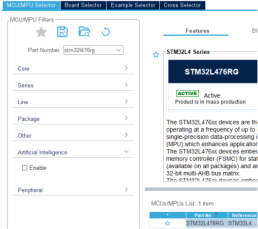
- File → New STM32 project → select STM32L476RG
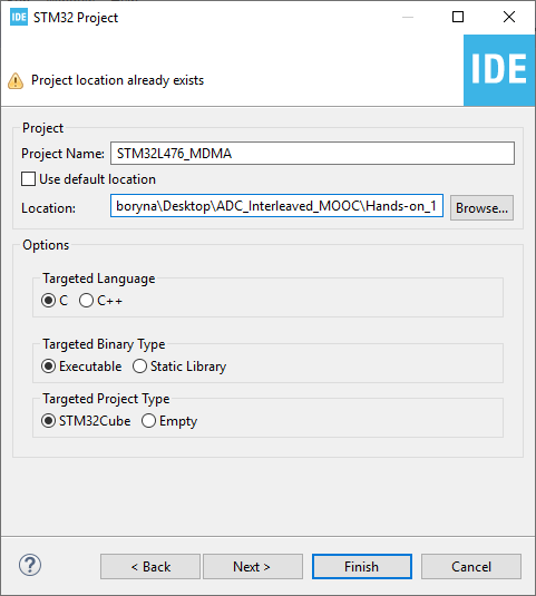
- Enter project name and location
- Press Finish button
 |  |
2. System Core
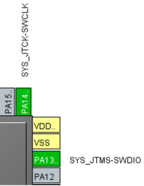
File → New STM32 project → STM32L476RG (NUCLEO)Pinout & Configuration tab → System Core → SYS
Select Debug interface: Serial Wire
 |  |
3. Analog Settings
- Pinout & Configuration tab → Analog → ADC1
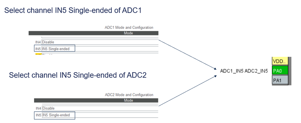
- Pinout & Configuration tab → Analog → ADC1 : ADC1 Parameters Settings tab:
-Mode: Dual interleaved mode only-DMA Access Mode: DMA access mode enabled-Delay between 2 sampling phases: 3 Cycles-Synchronous clock mode divided by 1-Continuous Conversion Mode: Enabled-DMA Continuous Requests: Enabled-Rank 1; Channel: Channel 5, Sampling Time: 6.5 Cycles
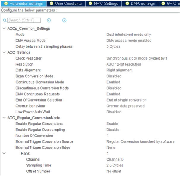
- Pinout & Configuration tab → Analog → ADC1: Configure ADC1 in DMA Settings tab
- ADC1, DMA1 Channel 1, Peripheral To Memory, Low
- Mode: Normal,
- Increment Address: Memory,
- Data Width: Word
- Increment Address: Memory,
- Data Width: Word
 |
 |
- Pinout & Configuration tab → Analog → ADC2 : Configure ADC2 in Parameters Settings tab
-Mode: Dual interleaved mode only
-DMA Access Mode: DMA access mode enabled
-Delay between 2 sampling phases: 3 Cycles
-Synchronous clock mode divided by 1
-Continuous Conversion Mode: Enabled
-Rank 1; Channel: Channel 5, Sampling Time: 6.5 Cycles
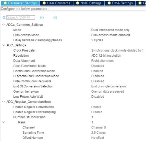
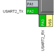
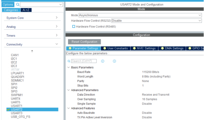
- Pinout & Configuration tab → Connectivity → USART2
USART2 Mode: Asynchronous
USART2 in Parameters Settings tab
USART2 in Parameters Settings tab
-Baud Rate: 115200 Bits/s,
-Char Length: 8Bits,
-Parity: None,
-Stop Bits: 1
 |  |
4. Clock Configuration tab
- Set HCLK frequency as 80MHz

5. Generate code
- Click on
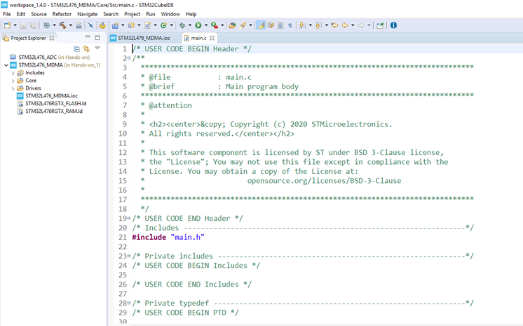
- Open C perspective and edit main.c file
6. Insert relevant code in main.c
- Follow user code section names, section by section and put relevant code of main.c
1. USER CODE Includes section

#include <stdio.h>
2. USER CODE PD

#define ADC_BUF_SIZE 20
3. USER CODE PV

static uint32_t adcBuf[ADC_BUF_SIZE];
static uint32_t adcFlag = RESET;
4. USER CODE 0

int _write(int file, char *ptr, int len)
{
 HAL_UART_Transmit(&huart2,(uint8_t*)ptr,len,100);
  return len;
}
5. USER CODE 2

HAL_ADCEx_Calibration_Start(&hadc1,ADC_SINGLE_ENDED);
HAL_ADCEx_Calibration_Start(&hadc2,ADC_SINGLE_ENDED);

LL_ADC_SetMultiDMATransfer(ADC123_COMMON,LL_ADC_MULTI_REG_DMA_LIMIT_RES12_10B);  //One shot MDMA mode

HAL_ADCEx_MultiModeStart_DMA(&hadc1,adcBuf,ADC_BUF_SIZE);
__HAL_DMA_DISABLE_IT(&hdma_adc1,DMA_IT_HT);  //Avoid DMA half transfer interrupt trigger
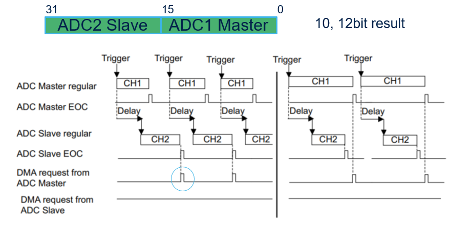
7. MDMA mode
- MDMA=0b10: a single DMA request is generated each time both master and slave EOC events have occurred, 32-bit register ADCx_CDR contains the two half-words representing two ADC-converted data items (10 or 12 bit).
- Follow user code section names, section by section and put relevant code of main.c
6. USER CODE 3

if (adcFlag)
{
  printf("-------------\r\n");
  for(uint32_t i=0;i<ADC_BUF_SIZE;i++)
  {
    printf("%u\r\n",(uint16_t)(adcBuf[i]&0x0000FFFF));  //LSB -> MASTER
    printf("%u\r\n",(uint16_t)(adcBuf[i]>>16));         //MSB -> SLAVE
  }
  HAL_Delay(1000);

  adcFlag = RESET;
  HAL_ADCEx_MultiModeStart_DMA(&hadc1,adcBuf,ADC_BUF_SIZE);
  __HAL_DMA_DISABLE_IT(&hdma_adc1,DMA_IT_HT);
}
7. USER CODE 4

void HAL_ADC_ConvCpltCallback(ADC_HandleTypeDef *AdcHandle)
{
  adcFlag = SET;
}


8. Final steps
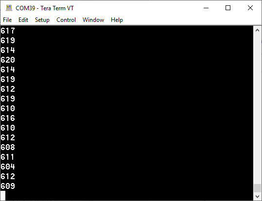
- 10. Start terminal: 115200,8,N,1 and observe ADC results, check if application is running
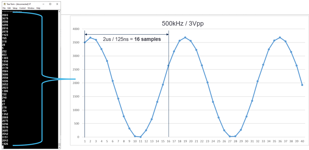
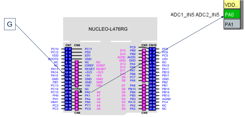
- 11. Connect signal generator: sinus 500kHz / 3Vpp, follow MCU electrical limits (unipolar voltage), pin 1 of CN8 or pin 28 of CN7
- 12. Observe the ADC results, import text data to Excel
Labels:

